This article mainly discusses the pulse test technology of semiconductor discrete device parameters. Here we can understand what is necessary for pulse test, what is its relevant standard, and what is the method of implementing pulse test.
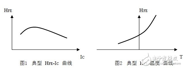
First, the necessity of pulse testingSemiconductor discrete devices usually include diodes, transistors, MOS transistors, junction transistors, thyristors, optocouplers and other devices. In the parameter test of these devices, it is necessary to first make the tested device meet the test conditions specified by the parameter test (ie, enter the specified working point), and also meet the specified test environment temperature, so that the measured data has actual significance. Because the parameters tested are both a function of the test conditions and a function of the ambient temperature. For example, the amplification factor HFE of the triode is both a function of the test conditions IC and VCE and is also very sensitive to ambient temperature. A typical HFE-IC curve is shown in Figure 1, and a typical HFE-temperature curve is shown in Figure 2.
However, in addition to the test conditions and ambient temperature will affect the parameter test, it is easy to be overlooked that the power consumed by the device under test under the test conditions will cause additional temperature rise on the device chip. The magnitude of the additional temperature rise depends on the power dissipated by the device under test under the specified test conditions, the time the power is maintained (ie, the test time), and the thermal resistance of the device under test. The larger the power dissipation, the longer the test time, and the greater the thermal resistance of the device, the greater the additional temperature rise of the chip. The reason why this is easy to be ignored is because they are in contact with the outer casing of the device under test, and it is difficult to know how high the temperature of the chip inside the tube is. This can only be known by testing and researching the thermal resistance of the device. What is the temperature rise curve of the device chip? The typical chip temperature rise curve is shown in Figure 3.
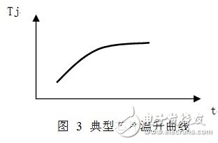
Since the initial stage of the temperature rise curve of the chip is steep and the heating rate is fast, the error of the test data caused by the additional temperature rise is often much more serious than people think, because in many cases the additional temperature rise of the chip is not a few degrees. It is more than a dozen degrees or even dozens of degrees. At this time, the test ambient temperature (especially the low temperature test) lost its practical significance.
In order to reduce the impact of the additional temperature rise, the only way is to shorten the test time. Because the test conditions of the parameters are standard, it is impossible to reduce the power consumption of the device by changing the test conditions. The thermal resistance of the device is also objective. Only the test time is shortened so that the additional temperature rise of the chip is negligible, so that the device under test The chip temperature is close to the specified test ambient temperature.
Second, the relevant standards for pulse testing requirementsSince the additional temperature rise of the device chip during parameter testing is a complex function of power dissipation, device thermal resistance, and test time, it is difficult to describe the dissipated power, device thermal resistance, and expected chip attach with a simple formula. In the case of temperature rise, it is reasonable to use how long the test time is. In order to unify the test requirements, the relevant standards specify the requirements for the pulse test and the recommended conditions.
1. US military standard MIL-STD-750C semiconductor device test method 4.3.2.1 provides:
When measuring static and dynamic parameters under pulse conditions, in order to avoid measurement errors due to device heating during measurement, the following provisions shall be specified in the detailed specification:
a. Mark the “Pulse Test†in the test specification.
b. Unless otherwise specified, the pulse time (tp) is 250-350 microseconds and the duty cycle is up to 2%.
2. National Military Standard GJB128-86 Semiconductor Discrete Device Test Method 3.3.2.1 Provisions:
In order to avoid test errors caused by device heating during measurement, when testing static and dynamic parameters under "pulse" conditions, it should be noted in the detailed specification:
a. The test should specify “Pulse Testâ€.
b. Unless otherwise specified, the pulse width should be 250-350μS and the duty cycle is 1-2%.
3. National standard GB/T 4587-94 (equivalent IEC 747-7-1988) In the specified conditions of the pulse test:
Pulse time and duty cycle (tp, δ), preferred: tp = 300μS, δ ≤ 2%.
4. National Standard GB/T 6218-1996 (equivalent IEC 747-7-3:1991) In the notes on the pulse test:
If using the pulse method:
Pulse duration and duty cycle (tp, δ) of the pulse signal source
Preferably: tp = 300 μS, δ ≤ 2%.
5. Generally, the collector-emitter saturation voltage drop VCE sat, the base-emitter saturation voltage drop VBE sat and the forward current transfer ratio HFE are specified in the transistor national military standard and the military standard specification (or blank specification). law. And clearly stated in the terms of the conditions of the pulse test:
The pulse test conditions shall be as specified in 3.3.2.1 of GJB 128.
The relevant provisions of the above standards are the so-called 300μS pulse test. According to the test and research on the thermal resistance of various semiconductor devices, the conditions of the 300μS pulse test are proved to be classic, which can guarantee the test in most cases. The temperature rise of the device chip is negligible.
Third, the method of implementing pulse testThe reason why the standard specification (or blank specification) of the standard specifies the pulse test for the parameters such as VCE sat, VBE sat and HFE is because the device will withstand large dissipated power when DC test is performed on the above parameters. In turn, the temperature of the device chip is raised, which affects the authenticity of the test data. If the test time is too long, the damage and damage of the device may be caused.
Different methods are used to implement pulse testing (especially HFE parameter testing) in different test systems. Commonly, there are two methods: software closed-loop method (see Figure 4) and hardware closed-loop method (see Figure 5).
Software closed loop method
The process of software closed-loop testing of HFE parameters is as follows:
a. Set the collector voltage source VCC (available with a programmable voltage source controlled by D/A) to bring the VCE to the specified voltage value.
b. Set the base current source IB (which can be implemented with a D/A controlled programmable current source) and read the value of the collector current IC (available with A/D).
c. Determine whether the value of the collector current IC meets the requirements specified in the test conditions (software judges).
d. Repeat the process of b and c (usually using a bitwise approximation) to bring the collector current IC closer to the requirements specified in the test conditions.
e. Read the value of the base current IB (the final set value of D/A) and calculate the value of the HFE parameter.
2. Hardware closed loop method
The hardware closed-loop method tests the HFE parameters as follows:
a. Set the collector voltage source VCC (available with a programmable voltage source controlled by D/A) to bring the VCE to the specified voltage value.
b. Compare the collector current IC and the IC value specified by the test condition (set by D/A) with a hardware comparator. The result of the comparison controls the base current source IBB, which in turn controls the collector current IC to automatically stabilize to the specified IC. value.
c. Read the value of the base current IB (A/D read) and calculate the value of the HFE parameter.
3. Comparison of the two test methods
According to the analysis and comparison of the test methods of the two methods, it can be seen that there are differences in the following aspects:
a. The control principle of the software closed-loop method is actually an improvement of the manual adjustment process of the direct current method, which is actually an open-loop control from the hardware point of view. The hardware closed-loop method is the principle of closed-loop feedback and automatic adjustment.
b. The software closed-loop method requires software intervention for each IB setting, and the IB settings must be modified several times to bring the IC close to the specified test operating point. Therefore, the entire control process takes a long time and cannot be stabilized within 300 μS. Test conditions and read data, usually takes several milliseconds, tens of milliseconds or even longer, so it does not meet the requirements of the relevant standards, and the device is hot due to long test time, which affects the authenticity of the data. The hardware closed-loop method can achieve stable test conditions and data reading in 300μS time, thus complying with the relevant standards, and the temperature rise of the device caused by the test time can be neglected.
c. The software closed-loop method is actually an open-loop control from the hardware point of view, so the collector current IC can only be close to the specified value. When the HFE data of the device under test is large (such as Darlington), the test There will be large deviations in conditions, which in turn will affect the accuracy of the HFE data. The hardware closed-loop method uses the principle of hardware comparison and feedback to ensure the accuracy of the test conditions and higher test accuracy for HFE.
d. The software closed-loop method is technically easier to implement because it is essentially open-loop control, and it is relatively difficult to generate parasitic oscillations. The hardware closed-loop method usually consists of a multi-stage amplifier and a device under test to form a closed-loop feedback system. If it is not handled well, it will easily generate parasitic oscillations.
4. Implementation of hardware closed-loop method
STS 2103A Semiconductor Discrete Device Test System The heart of the pulsed measurement line is a high-performance SM 2204E module (see Figure 6 for a simplified schematic of the HFE parameters). The module uses 14 operational amplifiers to form two identical functions. Four-phase limit precision measuring unit. Each measuring unit has the capability of constant voltage, constant current, pressure measurement and current measurement, and supports positive and negative voltages and currents to suit the testing of NPN and PNP devices. High-performance op amps and unique line design enable precision measurement cells with good frequency performance to meet 300μS pulse test requirements while delivering tens of amps of high current. After careful debugging and compensation, the module solves the problem of parasitic oscillation and makes the system have good test adaptability. At the same time, it also implements the Kelvin four-terminal method test until the pin of the device under test ensures high current. The accuracy of the parametric test allows the STS 2103A system to demonstrate good pulse test performance and comprehensive characteristics.
Fourth, STS 2103A semiconductor discrete device test system introductionSTS 2103A Semiconductor Discrete Device Measurement System is an intelligent two-level distributed test system designed and developed by Beijing Huafeng Measurement and Control Technology Co., Ltd. on the basis of digesting foreign systems and researching the needs and characteristics of domestic users. It is STS 2100 series electronic components. An important part of the test system, the company owns the independent intellectual property rights of the product.
The system is mainly suitable for transistor triode (NPN/PNP), diode (rectification, switching, detection, voltage regulation, etc.), VMOS (N-channel/P-channel), junction-effect transistor, thyristor, optocoupler and others. Semiconductor-like discrete devices.
The system conforms to the national standard, national military standard and military standard in the test principle and method, and adopts hardware closed loop for parameters such as collector-emitter saturation voltage drop VCE sat, base-emitter saturation voltage drop VBE sat and forward current transmission ratio HFE. The 300μS pulse test (pulse duty ratio 2%) can effectively suppress the temperature rise of the device chip caused by the test. Even if the test is performed under hundreds of watts of power, it will not cause the device to heat up, thus ensuring the authenticity and stability of the test data. Sex, while also ensuring the safety of the device under test.
The system uses the Kelvin bridge four-terminal method for parameter testing. All test sockets are tested by the US 3M company's imported four-terminal test socket, which effectively deducts the contact voltage drop of the system and contact links, ensuring the authenticity of the large current parameter test. And precision. For example, for the test of the saturation voltage drop of the triode, for the test of the on-resistance of the VMOS device, the test for the forward voltage drop of the diode (especially the Schottky diode) has the same high test even if the current is as large as several tens of amperes. Precision.
The system uses hardware closed-loop pulse mode to test HFE parameters, but at the same time has good test adaptability, from low-frequency tubes to ultra-high frequency tubes of up to several gigabits, from tens of milliwatts of low-power devices to several hundred watts. High-power devices, systems have good test performance.
The system low-voltage measuring unit has a basic test accuracy of 0.25%, which ensures that the system still has a comprehensive accuracy of better than 1% when measuring HFE parameters, in accordance with the 1% requirement for the measurement static parameters in GJB 128A-97. The system measures the resolution of the HFE parameter to 0.1, and has good stability. The small temperature rise of the device casing caused by hand insertion and removal of the device during the test leads to small changes of the device HFE parameter several times, and the system can be sensitive and stable. The ground is displayed.
While displaying the test data, the system also has the function of displaying the characteristic curve on the same screen, so that not only the accurate test data can be read on the screen, but also the breakdown characteristic curve and the output characteristic curve of the device can be visually seen, which is concerned about It is especially convenient for users who break through the shape of the characteristic curve and the uniformity of the output characteristic curve.
The system uses high-quality components and materials, digital analog high-voltage power supply technology, flow-measuring ground technology, equipotential ring technology, electrostatic shielding technology, software processing technology, using suspended wire and three anti-treatment processes, so that the system has a good Weak signal detection capability allows accurate testing of nanoampere currents even in wet conditions.
The STS 2103A Semiconductor Discrete Device Test System has excellent overall performance and is an ideal means of detecting the quality of discrete semiconductor devices.
Gfci Outlet,Gfci Socket,Gfci Plugs,Outdoor Gfci Outlet Box
Lishui Trimone Electrical Technology Co., Ltd , https://www.3gracegfci.com