Abstract: In order to meet the requirements of high bandwidth and large capacity in high speed image data acquisition system, a design method of DDR3 SDRAM controller user interface based on Verilog-HDL language is proposed by using Virtex-7 series FPGA external DDR3 SDRAM design method. . The controller user interface has been functionally verified on the Xilinx VC707 development board and successfully applied to high-speed image data acquisition systems. The controller with the user interface has the advantages of high bandwidth utilization, high portability and low cost compared with the general controller interface, and can be flexibly applied to different projects according to the needs of the designer.
With the rapid development of modern science and technology, in the fields of industrial production and scientific research, such as satellite communication and high-speed image processing, there are widespread processing requirements for high-speed, large-capacity, real-time and high-bandwidth data [1, 2]. . As a core part of each system, high-speed data acquisition systems are increasingly demanding data processing speed, real-time performance, stability, and power consumption.
At present, among the memory solutions capable of meeting both high bandwidth and large capacity requirements, mature DDR, DDR2, DDR3, etc., among which DDR3 has higher bandwidth and lower power consumption, thus becoming a high-speed real-time data storage system design. The preferred scheme [3]. Since DDR3 memory cannot directly recognize the processor's access request, it is necessary to design a controller to control the normal read and write operations of DDR3.
Compared to Virtex-6 series FPGAs, Virtex-7 series FPGAs have doubled system performance, reduced power consumption by half, increased memory bandwidth by a factor of 2, and have a unique IP core mig_v1. 7, which can be used to solve DDR3. Some complicated problems with memory. Therefore, based on the working principle of DDR3, this paper combines the IP core MIG_v1. 7, and gives a method to design the user interface of DDR3-SDRAM controller using Verilog-HDL language, and proposes a high-speed image data acquisition. The application of DDR3 memory in the system is also implemented on the Virtex-7 series of FPGAs.
1 DDR3-SDRAM technical characteristics The DDR3-SDRAM used in this paper is Micron's MT8JTF12864HZ-1G6G1 memory module. The DDR3 memory bank has 1 GB of memory and consists of 8 memory chips with a capacity of 128 MB. The data bit width of each chip is 8 bits, the row address lines are multiplexed by 14 lines, the column address lines are multiplexed by 10, and the number of banks is 8. Therefore, the capacity of each memory chip is 16 384 &TImes; 1 024 &TImes; 8 &TImes; 8, which is 128 MB. The eight slices together form the 64-bit data width of the MT8JTF12864HZ-1G6G1 with a capacity of 1 GB.
The control command signals of DDR3 mainly include chip select signal CS, row address select signal RAS, column address select signal CAS and WE write enable signal, and various operation instructions of DDR3 are substantially determined by the combination of these four signals. As shown in Table 1. Where H is high and L is low.
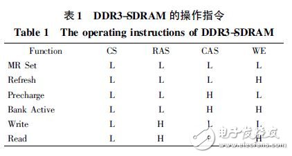
Table 1 DDR3-SDRAM operation instructions
There are four Mode Registers for DDR3, MR0, MR1, MR2 and MR3. When the four control command signals are low, the mode register can be selected by the Bank select bit. The Refresh operation is divided into Auto Refresh and Self. There are two kinds of Refresh, no matter what kind of refresh mode, no external row address information is needed, because this is an internal automatic operation; when DDR3 reads and writes, the memory will give a DQS signal synchronized with the data. It is used to accurately distinguish each transmission period in one clock cycle, which improves the accuracy of receiving data by the receiver.
Compared with the previous generation of memory devices, the memory mode of DDR3 has been greatly improved: the number of logical banks has been increased from 4 to 8 in DDR2; the burst length has been increased to 8 bits, and any burst interrupt operation will be in DDR3 memory. It is banned and not supported; it is replaced by a more flexible burst transfer control; its core operating voltage is reduced from 1.8 V of DDR2 to 1.5 V [4], which can achieve high bandwidth while Significantly reduce its power consumption; DDR3 uses FLY_BY bus, reference voltage separation, ZQ calibration function is added, which greatly improves the integrity of the stored signal; and DDR3 is green package, does not contain any harmful substances, reduces air Pollution.
2 DDR3-SDRAM controller user interface design
The design of the DDR3 controller adopts the design method of the IP core MIG_v1. 7 + user interface module introduced by Xilinx. This design mainly describes the user interface module. Figure 1 shows the overall implementation of the DDR3 controller.
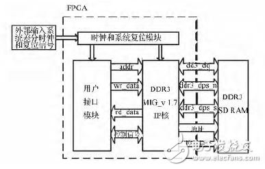
Figure 1 Overall implementation of the DDR3 controller
2. 1 User Interface Module Design The user interface module is the core module of the entire DDR3 controller system, which mainly includes the write data path and the read data path. Figure 2 shows the implementation of the user interface design of the DDR3 controller.
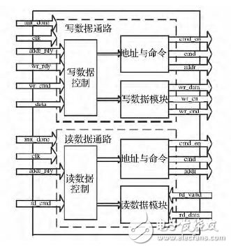
Figure 2 User interface design of DDR3 controller
At the input of the write data path, addr_rdy, wr_rdy, and init_done feed back the signal to the write data control module for the DDR3 IP core. When init_done is high, DDR3 has completed initialization, and when addr_rdy is high, it indicates DDR3 preparation. It is good to receive the write data address and write data commands. When wr_rdy is high, DDR3 is ready to receive write data; wr_cmd is write data command signal. At the output of the write data path, cmd_en is the enable signal for the command and address input to the DDR3 IP core, and wr_en and wr_end are the write data control signals input to the DDR3 IP core, aligned with the valid write data signal.
In the design of the user interface, the back_to_back read/write design mode is adopted. Addr_rdy, cmd_en, cmd and addr are used as the address bus, and wr_rdy, wr_en, wr_end and wr_data are used as the data bus. The two buses are independent of each other, and two feedback signals are used. Addr_rdy and wr_rdy are also relatively independent. At the beginning of the write data, ensure that the address bus advances the data bus one cycle. In the ideal case where addr_rdy and wr_rdy are not back-pressured, the write data is delayed by one cycle than the write address and write command. When addr_rdy and wr_rdy have When back pressure, the write data and the write address may not be satisfied by one cycle being issued.
The read data path is similar to the write data path design, where rd_valid is the read data valid signal and rd_data is the read data signal. In the read data path, addr_rdy, cmd_en, cmd, and addr are used as the address bus, and rd_valid and rd_data are used as the read data bus.
2. 2 The clock module of the user interface is designed to input a 200 MHz delayed reference clock and a 200MHz differential input clock. These input signals can generate the entire DDR3 controller and all clocks for DDR3 operation, including the user, through the clock and system reset module. The working clock of the interface, the working clock of the DDR3 IP core, and the clock of DDR3 read and write data. This design method has the advantage of simplifying the design structure of the controller and facilitating the management of the clock [5]. Figure 3 shows the implementation model of the clock module.
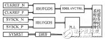
Figure 3 Clock and System Reset Module
3 DDR3-SDRAM controller user interface simulation
The operation of DDR3-SDRAM must be carried out according to certain rules and must comply with the corresponding state machine conversion requirements. Figure 4 shows the state machine for DDR3 memory operation. This state machine describes the conversion of each state of DDR3 and some of the involved in the conversion. command. The design of the DDR3 controller is essentially designed around the state machine to ensure that every DDR3 on the memory module is working properly.
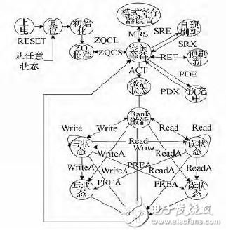
Figure 4 state machine for DDR3 memory
3. 1 Chipscope simulation result analysis of the user interface design module In this design, the hardware simulation uses the controller containing the user interface module to download to the Virtex-7 series FPGA, and observes the internal signal of the user interface in real time through Chipscope. . And in Figure 6, addr adds 1 every other clock cycle.
3. 2 Modelsim simulation results analysis of the user interface design module In this design, the software simulation uses the combination of ISE 14. 3 and Modelsim10.0a.
Figure 5 is an internal signal observation diagram of the user interface input signals addr_rdy and wr_rdy in the ideal case without back pressure. In this state, cmd_en is pulled higher than wr_en and wr_end one cycle ahead, and the effective address is correspondingly valid. There is a one-cycle time delay between the data. Figure 6 shows the internal signal observation of the user interface when the addr_rdy and wr_rdy signals are back pressure. In this state, the initial time cmd_en is pulled higher than wr_en and wr_end one cycle, and the effective address is different from the corresponding valid data. The time delay of one cycle, but after addr_rdy and wr_rdy are pulled low, the time delay of one cycle is no longer satisfied between the effective address and the corresponding valid data. Because the back-to-back mode is used in this design, the address bus and the data bus are independent of each other, so even if the effective address and the corresponding valid data no longer satisfy the time difference of one cycle, it will not affect the data. Transmission. In this mode, the transmission of data and address is more flexible, the control is more convenient, and the loss of data is effectively avoided.
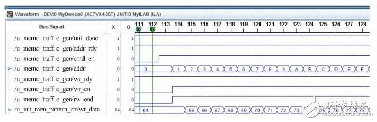
Figure 5: Internal signal observation of the addr_rdy signal and wr_rdy signal without back pressure
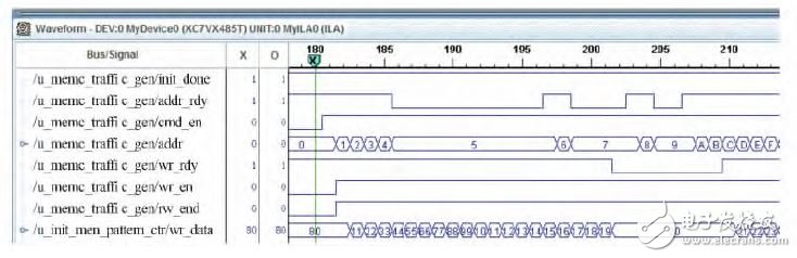
Figure 6 Internal signal observation of the addr_rdy signal and wr_rdy signal with back pressure
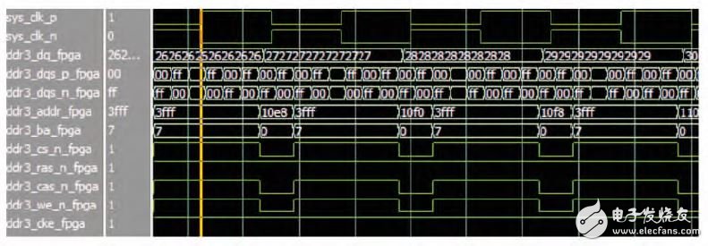
Figure 7 Modelsim simulation of writing data
Since DDR3 uses the burst transfer length BL = 8, the read and write address values ​​are continuously incremented by 8 so that the lower 3 bits of addr will always be 0, so when using Chipscope to observe the address, it is the 4th from addr. As the bit begins to observe, Figure 5 appears.
Since the memory core frequency used in this design is 200MHz, and because the memory bus number of DDR3 is 64 bits, DDR3 can pre-read 8 bits at a time, according to the memory bandwidth = memory core frequency &TImes; memory bus digits × multiplication Coefficient, so the memory bandwidth of DDR3 can reach 12. 5 GB and the transfer rate can reach 1 600 MB / s without considering the bandwidth occupied by operations such as refresh and activation. At such a fast transfer rate, it is difficult to observe the data written by the DDR3 controller into the DDR3 using Chipscope. Therefore, in this design, the DDR3 model is added to the DDR3 controller project in ISE 14.3, and the simulation of the DDR3 controller and the DDR3 model by Modelsim is used to observe the data written by the controller into the DDR3. .
As can be seen from Figure 7, the dq synchronization signals qds_n and dqs_p are changed 8 times in one clock cycle, that is, the write data is written 8 times in 64 bit units in one clock cycle. After the data transmitted by the user interface passes through the DDR3 IP core, it can be accurately written into DDR3. When reading data, it also reads 8 64-bit data in one clock cycle in 64-bit units.
3. 3 DDR3 controller user interface in high-speed image data acquisition system DDR3 controller with this user interface has been successfully applied to a high-speed image data acquisition system, Figure 8 is collected by the high-speed image data acquisition system picture of.
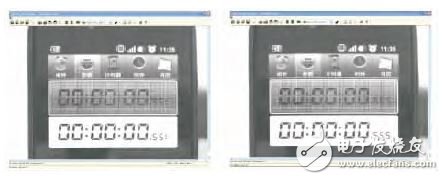
Figure 8 High-speed image data acquisition results
The image acquisition system sets the CMOS camera to operate in dual channel mode with 8 bit width and frame rate of 250 frames/s with a resolution of 2 040 × 1 024. The acquisition system passes the received image data through the DDR3 buffer, transmits it to the PC through the Gigabit Ethernet interface, and displays the data written in the PC as a picture. Figure 8 shows the two frames captured continuously by the acquisition system. It can be seen from the figure that the time interval between the two frames is 4 ms, which satisfies the frame number requirement, and the image is clear and complete, reaching the expected standard.
4 Conclusion The hardware platform of this design is Xilinx's Virtex-7 FPGA VC707 evaluation kit. The 7 Series FPGAs offer smaller size, lower cost, cost-effective and large capacity, and ultra-high-end connection bandwidth than the 6 Series and 5 Series FPGAs.
The user interface of the memory controller is designed to manage DDR3 memory modules well, and to complete various requests sent by users, and to maximize the speed and bandwidth of accessing memory, avoiding data loss, and successful. Applied to a high speed image acquisition system. The memory controller designed on the basis of this user interface can be compatible with most mainstream memory on the market, and is highly portable, which greatly reduces development costs.
ZGARVAPE
Zgar 2021's latest electronic cigarette Aurora series uses high-tech temperature control, food grade disposable pod device and high-quality material.Compared with the old model, The smoke of the Aurora series is more delicate and the taste is more realistic ,bigger battery capacity and longer battery life. And it's smaller and more exquisite. A new design of gradient our disposable vape is impressive. We equipped with breathing lights in the vape pen and pod, you will become the most eye-catching person in the party with our atomizer device vape.
The 2021 Aurora series has upgraded the magnetic suction connection, plug and use. We also upgrade to type-C interface for charging faster. We have developed various flavors for Aurora series, Aurora E-cigarette Cartridge is loved by the majority of consumers for its gorgeous and changeable color changes, especially at night or in the dark. Up to 10 flavors provide consumers with more choices. What's more, a set of talking packaging is specially designed for it, which makes it more interesting in all kinds of scenes. Our vape pen and pod are matched with all the brands on the market. You can use other brand's vape pen with our vape pod. Aurora series, the first choice for professional users!
We offer low price, high quality Disposable E-Cigarette Vape Pen,Electronic Cigarettes Empty Vape Pen, E-cigarette Cartridge,Disposable Vape,E-cigarette Accessories,Disposable Vape Pen,Disposable Pod device,Vape Pods OEM vape pen,OEM electronic cigarette OEM e-cigarette OEM e-cig to all over the world.


E-Cigarette Vape Pen,Disposable Device Vape,Vape Pen Atomizer,Latest Disposable E-Cigarette OEM vape pen,OEM electronic cigarette
ZGAR INTERNATIONAL TRADING CO., LTD. , https://www.szvape-pen.com