1 Introduction
In recent years, with the decline of manufacturing costs and the breakthrough of technical bottlenecks such as luminous efficiency and light decay, China's LED lighting industry has entered an accelerated development stage, and the application market has grown rapidly, which has led to a huge market for LED packaging products. Thousands of LED packaging companies have made China the largest producer of LED packaging in the world. The annual output value of LED packaging products has grown from 9.9 billion in 2004 to 14 billion in 2006 to 185 in 2008. 100 million yuan, and the annual output has exceeded one trillion [1] [2]. If the scrap/defective rate of the LED package is 0.1%, hundreds of millions of scrap/defective products may be generated in the trillions of LED packaging products per year, resulting in a direct economic loss of nearly 100 million yuan.
In order to ensure the quality of the package, LED packaging companies ensure the quality of the LED package by microscopic inspection and post-packaging inspection. The microscopic inspection before encapsulation is to perform manual visual inspection on the raw material chip with a microscope before packaging, to observe whether the surface of the chip material has mechanical damage and pitting, whether the chip size and electrode size meet the process requirements, and whether the electrode pattern is complete, and Eliminate the unqualified chips, avoid them from flowing into the next process, and produce defective products. After the package is finished, the optical and electrical parameters of the packaged products are inspected by the automatic spectrophotometer after the package is completed, and the test results are divided according to the test results. File, then package. Obviously, the microscopic inspection and the post-packaging inspection before packaging can only distinguish the defective products produced in the package from the genuine products, or divide the genuine products according to the parameters, and cannot improve the yield of the packaging.
For modern fully automated packaging lines, any small differences in their own will quickly have a direct impact on the quality of the packaged product. Therefore, under the condition that the fully automatic packaging line is widely popularized, the online real-time detection of the package quality actively in the packaging production process has become an inevitable requirement for improving the packaging level and ensuring the package quality. Due to the small size of the LED chip, high packaging process requirements, and fast package production, it is difficult to perform real-time quality inspection and control during the packaging process.
2. Analysis of the characteristics of LED packaging process
To perform real-time online inspection of the chip/package quality during the LED packaging process, it is necessary to first understand the process characteristics of the LED package and the parameters of the LED.
2.1 LED packaging process
The task of the LED package is to connect the outer leads to the electrodes of the LED chip while protecting the LED chips and to improve the efficiency of light extraction. The LED package is available in a variety of styles, depending on the application. The stent-type all-epoxy encapsulation is currently the largest and highest-yield form, so it should also be the key breakthrough target for on-line inspection of LED package product quality.
The main process of the stent-type full epoxy encapsulation is [4]. First, the LED chip is microscopically inspected and expanded, and in the center of the reflective bowl of each LED bracket and the back electrode of the chip in a set of connected stent rows. Silver glue (ie dispensing, glue preparation process) is spotted, and then the LED chip is sucked up by the vacuum nozzle to be placed at the center of the reflective bowl of the bracket, and the back electrode of the chip is fixed to the bracket by sintering (ie Solid crystal process); lead electrode lead is led to the LED chip by pressure welding to complete the connection work of the inner and outer leads of the product (ie, the pressure welding process); the optical epoxy glue is vacuum defoamed and then poured into the LED forming mold, and then the bracket is placed The whole is pressed into the LED molding die (ie, the potting process), the epoxy glue is cured at a high temperature, the annealing is cooled, the mold is demolded after curing (ie, the curing process), and finally the ribs of the LED bracket are cut off (shown in FIG. 1), and finally Carry out inspection and packaging.
2.2 Analysis of the characteristics of LED packaging process
From the packaging process of the LED, in the expansion, preparation, and crystallization of the chip, it is possible to damage the chip and affect all the optical and electrical characteristics of the LED; in the process of die bonding and pressure welding of the stent , there may be chip misalignment, poor internal electrode contact, or external electrode lead soldering or soldering stress, chip misalignment affects the distribution and efficiency of the output light field, and poor contact between internal and external electrodes or virtual soldering will increase the contact of the LED. Resistance; in the potting and epoxy curing process, bubbles and thermal stress may be generated, which may affect the output light effect of the LED.
Therefore, it can be known that both the LED chip and the packaging process have an influence on its optical and electrical characteristics, so the final quality of the LED is a comprehensive reflection of each process. In order to improve the quality of its packaging products, it is necessary to carry out real-time testing and adjustment of process parameters in various production processes to control defective products and waste products to a minimum.
Due to the fine, complex, high-speed characteristics of the packaging process, conventional contact measurement is almost impossible to achieve quality inspection in the package, and non-contact measurement is the most promising means.
3. The basic principle of non-contact detection
3.1 Photovoltaic characteristics of LED chips
The core of the LED chip is a doped PN junction. When a forward operating voltage VD is applied to it, the holes in the valence band are driven through the PN junction into the N-type region while the electrons in the conduction band are driven across the PN junction. Entering the P-type region, excess carriers will recombine near the junction, illuminate during the recombination process, and convert electrical energy into light energy. The property of illuminating under current driving conditions is determined by the doping characteristics of PN, and the photoelectric characteristics of photodiode PD are also determined by the doping characteristics of PN, so LEDs and PDs are similar in nature, so When the light beam is irradiated onto the open LED chip, photo-generated carrier electrons and holes are accumulated at both ends of the PN junction of the LED chip to form a photo-generated voltage VL. If the external circuit of the LED chip is short-circuited, the photo-generated carriers at both ends of the PN junction will directional flow to form the photo-generated current IL: [4][5]

Where: A is the PN junction area of ​​the chip, q is the electron charge, w is the barrier region width of the PN junction, Ln, Lp are the diffusion lengths of electrons and holes, respectively, and β is the quantum yield (ie, one photon per absorption) The number of electron-hole pairs generated, P is the average light intensity (i.e., the number of photons absorbed per unit area by the semiconductor material per unit time). They are:
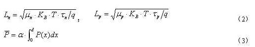
Among them, μn and μp are electron and hole mobility (related to the material itself, doping concentration and temperature), KB is Boltzmann constant, T is Kelvin temperature, and τn and τp are electron and hole loading, respectively. The lifetime of the flux (related to the material itself and temperature), α is the material absorption coefficient of the semiconductor PN junction material itself, the doping concentration and the wavelength of the excitation light, d is the thickness of the PN junction, and P(x) is within the PN junction. The intensity of the excitation light at position x.
It can be seen from the investigation formulas (1) to (3) that the photovoltaic characteristics of the LED chip are related to the structural parameters and material parameters of the PN junction, and these parameters are precisely the key parameters determining the LED illumination characteristics, so if the illumination characteristics of one LED chip are good Then its photovoltaic characteristics are good, and vice versa. Therefore, the intrinsic relationship between the light-emitting characteristics of the LED chip and the photovoltaic characteristics can be utilized, and the light-emitting characteristics of the LED chip can be indirectly tested by testing its photovoltaic characteristics, and the quality of the LED chip can be judged to achieve non-contact detection of the package quality.
3.2 Equivalent circuit of LED photovoltaic characteristics
For the LED of the bracket package, a set of ribbed brackets are clamped on the packaging machine during the packaging process, and then the chip and the bracket are packaged together to form the bracket package structure shown in FIG. It can be seen from Fig. 1(b) and (c) that the LED bracket, the bracket rib, the lead, the silver glue and the LED chip together constitute a complete external circuit shorting channel, which is in line with the working requirements of the photovoltaic effect. For the conventional detection method of LED package quality, such working conditions are completely impossible to detect.
Since the actual LED is not a pure ideal PN junction, it not only contains the internal resistance of the PN junction, the parallel resistance and the series resistance, but also includes the bracket, the bracket connection, the lead, the silver glue, so the PN junction is generated under external illumination. The photo-generated current IL formed by the photovoltaic effect is not exactly equal to the photo-generated current IL1 flowing through the stent. Therefore, the current flowing through the bracket is a comprehensive reflection of the photoelectric parameters of the LED.

If the internal resistance RL of the lead frame is regarded as the load of the LED during illumination and the photo-generated current IL generated by the PN junction photo-voltaic effect is regarded as a constant current source, the equivalent circuit of the LED when illuminated is as shown in FIG. 2 . That is, the LED operating under the photovoltaic effect can be equivalent to an ideal current source IL, an ideal diode D, and corresponding equivalent series and parallel resistances Rsh, Rs.
Features
â—† Designed For Water and Dust Tight(IP67)
â—† Small Compact Sizeâ—† UL&ENEC&CQC Safety Approvals
â—† Long life & high reliability
â—† Variety of Levers
â—† Wide Range of wiring Terminals
â—† Wide used in Automotive Electronics,Appliance and Industrial Control etc.
â—† Customized Designs
Micro Lever Switch,Enec Micro Switch,Ip67 Rotary Switch,Snap Action Micro Switch
Ningbo Jialin Electronics Co.,Ltd , https://www.donghai-switch.com