The driving methods of the liquid crystal display include: a static driving method, a dynamic driving method, and a dual-frequency driving method. This article only explains the most widely used dynamic driving method. Taking the dot-matrix liquid crystal display as an example, its dynamic driving method is introduced, and a method to overcome the crossover effect is given.
The liquid crystal display is due to the application of an electric field on the display pixel. This electric field is the synthesis of the potential signals on the two electrodes before and after the display pixel. Since a DC electric field easily reduces the lifespan of liquid crystals, generally only an AC electric field with a very small DC component is established. The DC component is usually less than 50mV. The driving of the liquid crystal display establishes a driving electric field by adjusting the phase, peak value, frequency, etc. of the potential signal applied to the electrodes of the liquid crystal display to achieve the display.
Dynamic drive
When the LCD displays a large number of pixels, such as a dot matrix type, in order to save a huge hardware drive circuit, the manufacturing and arrangement of the LCD electrodes are processed, and a matrix structure is implemented: that is, the back electrodes of a horizontal group of display pixels are connected Leading together, called row electrodes; connecting the segment electrodes of vertical display pixels together, called column electrodes. Each pixel on the display is uniquely determined by its row and column. The dynamic driving method of the liquid crystal display is to cyclically apply a selection pulse to the row electrodes, and at the same time to add a corresponding selective or non-selective driving pulse to all the column electrodes, thereby realizing the display function of all pixels in a row. This scanning is carried out in a row-by-row sequence, with a short cycle period, which results in a stable image on the LCD screen.
The selection time of each line in a frame is equal. Assuming that the number of scanning lines in one frame is N and the scanning time is 1, then the selection time occupied by one line is 1 / N of one frame time. This is the duty cycle coefficient of the liquid crystal display drive, also known as the duty cycle.
Overcome cross-effects
In the dynamic drive mode, to display a position such as (i, j) point, it is necessary to apply a selection voltage to the i-th column and the j-th row at the same time to maximize the variable electric field strength at this point, but at this time except In addition to point (i, j), the remaining points in the i-th column and the j-th row are also subjected to a certain voltage. These points are called semi-selected points. If the effective voltage at the half-selected point is greater than the threshold voltage, an undesirable display will appear on the screen, causing the contrast to decrease. This is the crossover effect. The method to solve the cross effect is the average voltage method, which is to average the voltages of the semi-selected points and the non-selected points, and moderately increase the voltages of the non-selected points to offset part of the voltages at the semi-selected points, so that the voltage at the semi-selected points drops, Increase display contrast. This is illustrated by Figure 1:
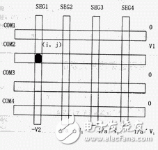
The selection point in Figure 1 is (SEG1, COM2), hereinafter referred to as (1, 2). The V1 voltage is applied to the second row, and the remaining row voltage is 0V; the -V2 voltage is applied to the first column, and the rest are non-selected voltages 1 / a'V1. Next, the potential difference at each point is analyzed, that is, the row voltage minus the column voltage.
Selection point: (1, 2): V1 + V2
Semi-selected points: (1,1), (1,3), (1,4): V2 (2,2), (3,2), (4,2); V1-1 / a'V1
Non-selected point: -1 / a'V1
To ensure the display effect of the selected point, keep V1 + V2 = VLCD at the required voltage value VLCD. At the same time, in order to improve the contrast of the display, let | V2 | = | -1 / a'V1 |, namely:
![]()
Solution:
![]()
Let: a '+ 1 = a, get:
![]()
Therefore, the voltage at each point in Figure 1 is:
Selection point: (1, 2): VLCD
Semi-selected points: (1, 1), (1, 3), (1, 4): (1 / a) VLCD (2, 2), (3, 2), (4, 2): [(a- 2) / a] VLCD
Non-selected points:-(1 / a) VLCD
It can be seen that the voltages at the line half selection point and the non-selection point are 1 / a of the display voltage VLCD. This 1 / a is called the bias coefficient, also known as the bias voltage. This method is called the 1 / a bias average voltage method, or simply referred to as the 1 / a bias method. In this method, MAX {[(A-2) / a] VLCD, (1 / a) VLCD} will become the scale to adjust the display contrast. When the number of scanning lines N = 1, the dynamic driving method is equal to the static driving method.
Application example of dynamic driving method
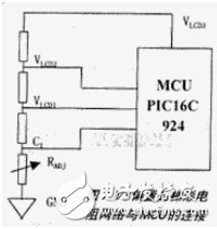
In the process of selecting the display method of the alcohol concentration detector, the author finally selected the VM807-2 type 8-bit code segment (7-segment) liquid crystal display produced by Hong Kong Jingdian Company through various investigations and investigations. This is not only because the LCD consumes a small amount of electrodes, but also because the MCU (PIC16C924) we use already has the driving capability of the LCD. Therefore, whether it is from the consideration of cost reduction or the simplification of the circuit, this choice is undoubtedly more reasonable of. Below we will explain the specific application of the LCD module in the MCU.
LCD module configuration
1. Configuration of LCDCON register
The LCDCON register is shown in Figure 2:
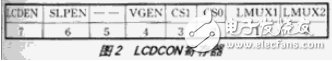
Among them: LCDEN: LCD module enable; SLPEN: sleep mode enable; VGEN: internal voltage generation enable; CS1: CS0: LCD clock selection bit, "00" = Fosc / 256, Fosc = 4MHz; LMUX1: LUMX2: public Terminal number and offset selection, "10" = 3 common terminal, 1/3 offset.
The configuration code I used is.
Configuration of LCDPS register
The LCDPS register is shown in Figure 3:
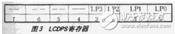
Among them: LP3: LP0 frame clock frequency division selection bit
The configuration code I used is: *** 0011, where "*" stands for "0" or "1".
According to the frame frequency calculation formula, the frame frequency is:
CLOCk source / 96 (LP3: LP1 + 1)
= 4 & TImes; 106/96 & TImes; (3 + 1) & TImes; 256
= 40.69Hz
2. Pixel control
The pixel is uniquely determined by the first status bit of the pixel register. The LCD module has a total of 16 pixel registers, which can control up to 4 & TImes; 29 = 116 pixels. The LCD we use has a total of 8 × 8 = 64 pixels. Therefore, the pixel data register is sufficient. The pixel data register of the LCD is shown in Figure 4:
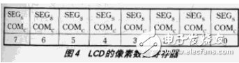
Bit 7: Bit 0: SEGSCOMC indicates the segment code and common number of the control pixel data. Among them, the subscript "S" means "0 ~ 32" segment codes, and the subscript "C" means "1 ~ 4" common terminals. A register bit of "1" means turning on the pixel (black); a register bit of "0" means turning off the pixel (bright).
3. Segment code enable
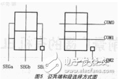
The segment code is enabled through the LCDSE register. Because VIM807-2 is an 8-bit 7-segment display, and we chose a 1/3 duty cycle (that is, 3 common terminals), therefore, the LCDSE register must select 3 × 8 = 24 segments to meet the needs, that is, the expression is completed All code segment pixels. Of course there will be excess, 8 × 9 = 72, because every 3 commons and 3 segments can express 9 pixels. The common terminal and segment selection methods are shown in Figure 5.
The LCDSE register is shown in Figure 6:
The meanings represented by you are the number of bits, pin function, the number of pin control segments at 3COM and the selected control segment. According to the above, the control code of LCDSE is.
4. Generation of LCD drive voltage
There are two methods for generating the LCD driving voltage, the internal charge pump method or the external ladder resistor network method. Since the LCD charge pump is in development, in order to reduce the design risk, we use a more mature external ladder resistor network method. When using an external ladder resistor network, VGEN (LCDCON "4") should be cleared.
5. LCD module configuration program
...
MAIN BCF STATUS, PRO
BSF STATUS, RP1
MOVLW 0X82
MOVWF LCDCON
}
MOVLW 0X03
MOVMF LCDPS
MOVLW 0X3B
MOVWF LCDSE
For diifferent USB types, micro USB, mini USB, etc. The logo, color or shape can all made as customers' requirement. With more than ten years of experience and capabilities assisting our customers in various industry, ETOP would be confident to be your qualified AVL and reliable manufacturing partner.
Related Products:usb cable,micro usb cable,usb data cable.
Data Cable,Data Flexible Electrical Magnetic Cable,Usb Data Cable,Micro Usb Cable,USB Connector
ETOP WIREHARNESS LIMITED , http://www.oemwireharness.com