Industrial Router Crystal 3.2*2.5mm 3225 26M (26.000MHZ) 12PF 10PPM 20PPM 30PPM
MOS Power IC Full Range
L0504-Murata muRATA Common Mode Inductor 90Ω 150mA
Supply 1206 Red and Green Two-Color LED, 1210 Red and Green Two-Color LED
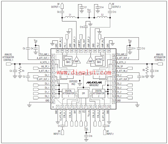
 Below is the circuit diagram of the **MAX2062 Dual Modulo VGA Application Circuit**.
The **MAX2062** is a high-performance dual variable-gain amplifier (VGA) that operates from 50 MHz to 1000 MHz. It offers a maximum gain of 19.4 dB, with a very flat gain response of 0.34 dB across a 100 MHz bandwidth. At 200 MHz, it provides 56 dB of isolation, making it ideal for applications requiring high signal integrity and minimal cross-talk.
This device includes an integrated 8-bit DAC, eliminating the need for external analog attenuation control. It runs on a single 5V supply, which simplifies power design. The MAX2062 also delivers excellent linearity, with a 41 dBm OIP3 at 200 MHz and 56 dBm OIP2. It has a 19 dBm input level at 1 dB compression, ensuring reliable performance even under high signal conditions.
It is commonly used in various communication systems, including:
- IF and RF Gain Stages
- Temperature-Compensation Circuits
- GSM/EDGE Base Stations
- WCDMA, TD-SCDMA, and CDMA2000 Base Stations
- WiMAX, LTE, and TD-LTE Base Stations and CPE
- Fixed Broadband Wireless Access
- Wireless Local Loop
- Military Systems
The MAX2062 is particularly well-suited for applications where precision, stability, and wide frequency range are essential. Its robust design and high performance make it a popular choice in both commercial and specialized communication infrastructure.
Below is the circuit diagram of the **MAX2062 Dual Modulo VGA Application Circuit**.
The **MAX2062** is a high-performance dual variable-gain amplifier (VGA) that operates from 50 MHz to 1000 MHz. It offers a maximum gain of 19.4 dB, with a very flat gain response of 0.34 dB across a 100 MHz bandwidth. At 200 MHz, it provides 56 dB of isolation, making it ideal for applications requiring high signal integrity and minimal cross-talk.
This device includes an integrated 8-bit DAC, eliminating the need for external analog attenuation control. It runs on a single 5V supply, which simplifies power design. The MAX2062 also delivers excellent linearity, with a 41 dBm OIP3 at 200 MHz and 56 dBm OIP2. It has a 19 dBm input level at 1 dB compression, ensuring reliable performance even under high signal conditions.
It is commonly used in various communication systems, including:
- IF and RF Gain Stages
- Temperature-Compensation Circuits
- GSM/EDGE Base Stations
- WCDMA, TD-SCDMA, and CDMA2000 Base Stations
- WiMAX, LTE, and TD-LTE Base Stations and CPE
- Fixed Broadband Wireless Access
- Wireless Local Loop
- Military Systems
The MAX2062 is particularly well-suited for applications where precision, stability, and wide frequency range are essential. Its robust design and high performance make it a popular choice in both commercial and specialized communication infrastructure.
(Editor: Circuit Diagram)
Dongguan Zhonghe Electronics Co., Ltd. , https://www.zhonghesleeving.com