The RF power amplifier is one of the core modules in the wireless transmitter and the most expensive module of the wireless transceiver. In order to reduce power consumption and extend battery life, it requires high efficiency and high power output. With the continuous improvement of silicon CMOS technology, high-performance power amplifiers using standard CMOS technology are the inevitable trend of today's RF circuits to smaller size, lower price and integrated chip integration. Researchers are involved in relevant theoretical research and A lot of work has been done on the improvement of circuit performance [1~5]. Based on the 0.18μm CMOS process, this paper designs and implements a two-stage fully integrated Class E switch mode power amplifier operating at 2.4GHz with good efficiency and integration.
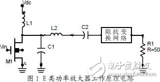
Figure 1 shows the circuit for the operation of a standard Class E power amplifier. Among them, the choke inductor L1 prevents the AC signal from passing through and provides DC current to the transistor. L2 and C2 form a series resonant network, so that the current flowing through the network is an ideal sinusoidal signal, and all harmonic components are filtered out. The parallel grounding capacitor C1 consists of two parts, one is the parasitic capacitance of the transistor and the other is the actually introduced capacitor. The drive voltage overdrive causes transistor M1 to be used as a switch. When it is turned on, the voltage drop across the transistor is zero; when it is turned off, the current flowing through the transistor is zero. Class E power amplifiers are shaped by the voltage on the switch, so that the voltage and voltage change slopes on the switch are almost zero when the switch is turned on, thereby reducing switching losses and improving efficiency. Usually the circuit component parameters can be roughly determined by the following formula [6]:
Where Q is the circuit quality factor, ω is the operating frequency, dc V and dc I are the drain voltage and current, and RL is the matching resistor obtained by impedance-transforming the terminal 50Ω resistor to obtain the required power out P.
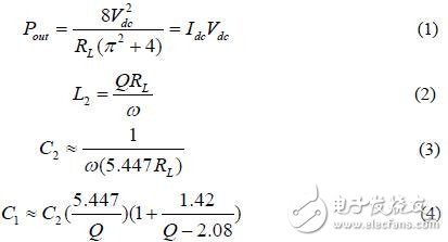
3 circuit design and analysisNormally, the gain of a single-stage power amplifier is only about 10 dB. It is necessary to increase the driver stage of high gain to increase the gain of the overall power amplifier. Therefore, power amplifier design is generally divided into power output stage, output matching, gain driver stage, inter-stage matching, input matching and other parts. Figure 2 shows the specific circuit of a two-stage fully integrated Class E switch mode power amplifier designed and implemented in 0.18μm CMOS process based on this structure idea. The driver stage is quasi-F type and the output stage is E class.
The power output stage uses the standard Class E power amplifier structure described in the operating principle. This common source structure consisting of M3 tubes can make full use of the amplitude of the power supply voltage and increase the output voltage swing. Since the maximum voltage at the drain of the Class E power amplifier may rise to 3.6Vd 2 [1], to ensure that the MOS transistor is not broken down, the circuit is powered by 2V. The power output stage is the most critical stage in the RF power amplifier. Its performance characteristics, including output power, efficiency, etc., will directly affect the performance of the entire amplifier. The transistor must be selected to provide at least dc I of DC current at the minimum voltage drop and operate in the linear region. At the same time, the output power and efficiency of the transistor must be scanned to ensure that the selected transistor meets the pre-designed performance specifications. Our experience in the design process shows that the output power and efficiency of the output transistor can be effectively predicted by Load-Pull technology, and these two indicators will be improved after the overall circuit design.
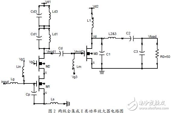
3.2 Output Matching NetworkUsually, the circuit terminal is connected to a 50Ω resistor. To achieve the desired output power, the actual load RL calculated by equation (1) is usually small and requires impedance transformation. The purpose of the output matching network is to provide the impedance required for maximum power transfer from the output of the device to the load impedance. In order to minimize passive components and effectively filter out higher harmonic components, the circuit uses the L-type low-pass impedance matching structure shown in the wireframe of Figure 3. In this way, the L-type low-pass impedance conversion circuit inductor L3 can be combined with the series resonant inductor L2 of the power output stage to form a single inductor L2&3, thereby effectively reducing the chip area occupied by the on-chip inductor. Due to the high operating frequency of the power amplifier, the parameters of the impedance characteristics of the transistor are affected by the operating frequency, the input level, the output load impedance, the power supply bias, and the temperature. The impedance of a power amplifier transistor is generally a complex number and will not only vary with frequency, but also with the voltage and current of the output signal, so that the impedance transformation network between the output stage and the antenna is compared. difficult. In the design, the output impedance transformation network uses Load-Pull technology to obtain the optimal load impedance, and then use the Smith graphic design tool to obtain the specific parameters of the low-pass impedance matching component according to the resistance.
The gain driver stage uses a cascode structure consisting of M1 and M2 plus a quasi-F-class amplifier mode composed of two resonant networks. The cascode structure can effectively reduce the influence of Miller capacitance and improve the isolation between input and output. In the two resonant networks: the resonators composed of Cd1 and L d1 are tuned at ω, and the resonators composed of Cd 3 and Ld 3 are tuned at 3ω. By properly tuning these four parameters, ensure that the resonant network is shorted to the second harmonic, and the output circuit is superimposed on the fundamental and third harmonics to obtain the approximate square wave drive signal required for the Class E amplifier. In the circuit performance test, we found that since the peak-to-peak value of the switching voltage of the quasi-F-type amplifier structure can reach 2Vd1, the power supply voltage of the gain-driven stage can be greatly reduced, thereby effectively reducing the DC power consumption of the entire circuit and improving the overall efficiency of the circuit. .
3.4 Inter-stage matching networkThe interstage matching network needs to match the output impedance of the previous stage device and the input impedance of the latter device. A high gain interstage topology should be selected and a flat gain response should be achieved. Inter-stage matching should also have a step-and-drain DC function, usually with a DC blocking capacitor Cd. The parallel inductance Lm of the circuit can reduce the parasitic capacitance Cm of the MOS transistor seen at the input of the power output stage, thereby improving the voltage transmission efficiency [5]. The interstage matching equivalent circuit is shown in Figure 4. The equivalent impedance seen from the output of the gain driver stage is:
The square wave signal of the gain driver stage is superposed by the fundamental wave and the third harmonic. Therefore, it is necessary to ensure that the third harmonic and the fundamental equivalent impedance seen by the output of the gain driver stage must have the same capacitance by the formula (5). Or inductive, otherwise the square wave cannot be formed due to the opposite phase. In addition, we also found that the Cd value is sensitive to the transmission efficiency. In order to improve the voltage transmission efficiency, Cd generally needs to take a larger value.
This design is based on the 0.18μm CMOS process, fully considering the on-chip inductor quality factor is not high, the inductance value is small and the occupied area is large, the whole chip integration is realized. The simulation was performed using the ADS2005A under the condition of 2V power supply voltage. The simulation results are shown in Figure 5.
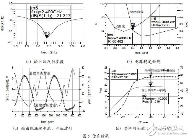
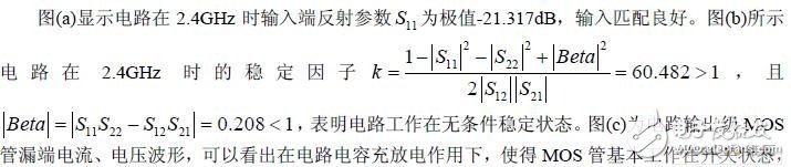
When the current Id approaches zero, the voltage Vd reaches a peak value, and when the current Id reaches a peak value, the voltage Vd tends to zero, which basically coincides with the output target of the ideal class E switch mode power amplifier, thereby achieving higher power and higher efficiency of the circuit. Output. Figure (d) shows that the output power of the circuit is about 21.5dBm at input power of -10dBm, and the power added efficiency is better than 57.69%. The corresponding power gain is 31dB.
In the performance simulation process, we found that the impedance matching of the circuit levels has a great influence on the circuit. Impedance matching is the key to the success of the circuit design. Using Load-Pull technology is an efficient and convenient way to get the best output matching load and predict transistor output power and efficiency. In addition, the size of the output transistor is closely related to the output power and efficiency of the overall circuit. The optimal size is available, so that the main performance of the circuit is optimized, but the corresponding working conditions of the circuit, such as the driver stage power supply voltage, are higher. Need to be compromised.
5 ConclusionThe innovation of this paper is that the parallel connection capacitor Cp between the gate and source of the input matching transistor greatly improves the flexibility of the chip inductor selection. At the same time, the quasi-F-class amplifier is used as the driver stage to obtain the required class of the class E power amplifier. Wave drive signal. The class E switch mode power amplifier designed in this paper achieves the goal of full integration, high efficiency and high power output, and achieves advanced level compared with domestic and foreign design [3-5]. With the continuous improvement of CMOS technology and inductor technology, the power amplifier realized by this technology will have broad application prospects in the future wireless communication field.
Solar Charge Controller Pwm,Outdoor Solar Charge Controller,Manual Solar Charge Controller,Intelligent Solar Charge Controller
GuangZhou HanFong New Energy Technology Co. , Ltd. , https://www.gzinverter.com