1 Introduction
With the development of electronic technology, in the fault detection of modern electronic products, a sinusoidal signal source whose frequency and amplitude can be automatically adjusted is often required, and the signal generated by the signal source is required to have good frequency stability, fast conversion speed, and frequency modulation. The function of amplitude modulation and phase modulation. Based on the actual needs, this paper proposes a design scheme of direct frequency digital synthesizer based on single chip microcomputer and FPGA, which can generate two sine wave signals with adjustable frequency and phase, which meets the predetermined requirements.
2. System design
2.1 System performance analysis
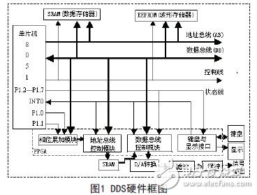
The system is mainly composed of the minimum system of MCU, memory circuit, FPGA module, keyboard and display interface circuit, D/A conversion circuit and low-pass filter circuit. The hardware block diagram is shown in Figure 1. The frequency control word, the phase control word and the amplitude control word are input through the keyboard. The minimum system control of the single-chip microcomputer generates the sine wave signal required by the user, and then undergoes DA conversion, and finally generates a smooth sine wave signal through the low-pass filter.
System performance requirements: frequency range 20Hz~20KHZ, step 20Hz; difference 0o~359o, step 1o; two output sine wave signals, peak-to-peak value varies from 0.3V to 5V; digital display frequency, phase difference.
2.2 Principles of system implementation
2.2.1 Basic principles of DDS
The basic principle of Direct Digital Synthesizer (DDFS):
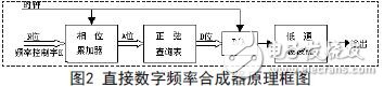
The DDS uses the sampling theorem to sample, quantize, and encode the sinusoidal signal according to the phase interval, and then store it in the EPROM to form a sinusoidal lookup table, and generate the waveform by looking up the table.
It consists of a reference clock, a phase accumulator, a sine lookup table, and a D/A converter, as shown in Figure 2.
The phase accumulator is composed of an N-bit adder and an N-bit accumulating register. The block diagram is shown in Figure 3. Each time a clock pulse Fc, the N-bit adder adds the frequency control data K to the accumulated phase data output from the accumulation register, and sends the added result Y to the input terminal of the accumulation register. The accumulating register feeds back the new phase data generated after the last clock cycle to the input of the adder, so that the adder continues to add the frequency control data K under the action of the next clock; The result of the addition forms the address of the sine lookup table, and the amplitude quantized sine function value in the cell corresponding to the phase in the table is taken out and sent to the amplitude/phase conversion circuit as the sample address value. In this way, the waveform sample value (binary code) stored in the waveform memory can be detected through the lookup table to complete the phase to amplitude conversion. The output of the waveform memory is sent to a D/A converter, which converts the amplitude of the waveform in digital form into an analog form signal of the desired composite frequency.
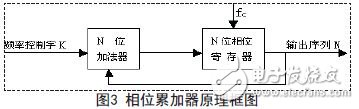
The maximum count length of the phase accumulator is the same as the number of phase separation points stored in the sinusoidal lookup table. When the sampling frequency (determined by the reference clock frequency) is constant, the phase increment of the phase accumulator is different, which will result in one cycle. The number of sampling points is different, and the frequency of the output signal changes accordingly.
If the initial phase of the accumulator is set, the output signal can be phase controlled. According to the sampling principle, if two identical frequency synthesizers are used and their reference clocks are the same, and the same frequency control word and different initial phase are set at the same time, then in principle, the output two channels can have a certain phase difference. The same frequency signal.
2.2.2 Direct Digital Synthesizer Implemented by FPGA
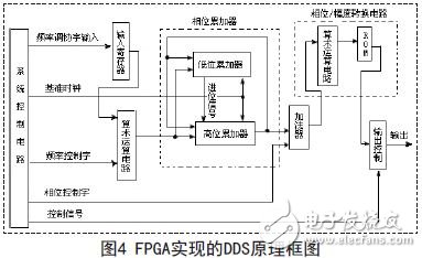
Based on the basic principle of DDS, the FLEX10 series devices of Altera's FPGA chip are used to convert the value of the waveform sampling point into analog output through digital-to-analog converter (MDAC), which can achieve the intended purpose and has high cost performance. The basic link consists of a counter, a read only memory (EPROM), a digital to analog converter (MDAC), and a filter.
The specific scheme is as follows: the accumulator is composed of an adder and a D flip-flop cascade, and under the control of the clock pulse fc, the input frequency control word K is accumulated, and an overflow occurs when the full amount is accumulated. The output of the phase accumulator corresponds to the phase of the composite period signal, and this phase is periodic and varies from 0 to 2Ï€. The number of phase accumulators is N, and the maximum output is 2N-1, corresponding to the phase of 2Ï€. When accumulating once, a corresponding phase code is output. The amplitude of the sinusoidal signal is obtained by looking up the table, and then D/A conversion and low-pass filtering are performed. The filter filters out unwanted sample components to output a spectrally pure sine wave signal. The circuit structure of the entire DDS circuit is shown in Figure 4.
3. System hardware circuit design
In terms of function, MCU and FPGA have strong complementarity.
The single-chip microcomputer has the characteristics of high cost performance, flexible function, easy man-machine dialogue, and good data processing capability; FPGA has the advantages of high speed, high reliability, convenient development and specification. The circuit architecture combined with these two types of devices will continue to be widely used in many high performance instrumentation and electronics.
The function of the MCU is mainly to transmit the frequency control word K1 and the phase control word K2 to the FPGA; the generated waveform table is stored in the EEPROM; the keyboard is written and the LED is displayed; and the DAC0832 is controlled for amplitude conversion. Before each power-on, it must be initialized by the MCU, the written program is loaded on the signal generation system, and then the data input from the keyboard is sent to the central processing chip, and the signal is output through the low-pass filter. The digital tube displays the frequency and phase difference of the signal.
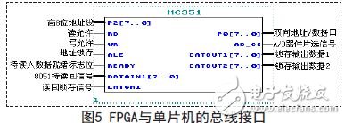
The bus interface between FPGA and MCU is shown in Figure 5.
1. An open structure of heating elements with half round stainless steel
reflectors for an optimal use of energy.
2. The Gyros will change direction automatice, if there is a force.
3. Removable and detachable parts for easy clean.
4. The particular broiling result is obtained by alternating heating and
cooling down. The meat fibres do not harden, and the gravy is flavoured
by the spices. This cooking mode results in very healthy meat.
5. The Vertical Grill allows broiling meat layers, shashlik, party sausages,
poultry and fish with few attachments.
6. The Skewers and Gyros go in opposite direction so that the food could
be heated more well.
7. Power: 1400W

Smokeless Electric Grill,Electric Multi Grill,Non-Stick Electric Grill,Electric Bbq Grill
Housoen Electric Manufacture Co., Ltd. , https://www.housoenappliances.com