The differential bridge sensor monitoring circuit with temperature compensation is a complete low power signal conditioner for bridge sensors, including a temperature compensation channel. This circuit is ideal for driving industrial pressure sensors and load cells with voltages between 5V and 15V. The article is a detailed introduction for everyone.
Function and advantageThe circuit shown in Figure 1 is a complete low-power signal conditioner for bridge-type sensors, including a temperature-compensated channel. This circuit is ideal for driving industrial pressure sensors and load cells with voltages between 5V and 15V.
With a built-in programmable gain amplifier (PGA) for 24-bit sigma-delta ADCs, the circuit can handle full-scale signals from approximately 10mV to 1V, making it suitable for a wide range of pressure sensors.
The entire circuit uses only three ICs and consumes only 1mA (not including bridge current). Ratiometric technology ensures that the accuracy and stability of the system is independent of the reference.
Low-power, temperature-compensated bridge signal conditioner and driver circuit
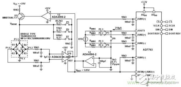
Figure 1. Differential bridge type sensor monitor with temperature compensation (schematic diagram: all connections and decoupling are not shown)
Circuit descriptionThe circuit shown in Figure 1 is based on the 24-bit Σ-Δ ADCAD7793. The ADC has three differential analog inputs and an on-chip low-noise PGA with a gain range of up to 128, making it ideal for multiple sensor interfaces. With a maximum power consumption of only 500μA, the AD7793 is suitable for low power applications. It has a low noise, low drift bandgap reference and an external differential reference. The output data rate can be set by software from 4.17Hz to 470Hz.
The AD8420 is a low power instrumentation amplifier with a supply current of up to 80μA and can be powered from a single supply up to 36V to eliminate the common-mode voltage of the bridge sensor. It also provides gain for the sensor's small differential signal output when needed.
The ADA4096-2 is a dual op amp with a typical supply current of 60μA per amplifier and a wide operating input voltage range of up to 30V for driving the sensor bridge. The other half of the ADA4096-2 is used as a reference voltage buffer.
There are many types of pressure sensors that require a voltage drive between 5V and 15V. The circuit shown in Figure 1 provides a complete solution for the bridge sensor with four key components: sensor voltage drive, instrumentation amplifier, reference buffer and ADC.
Bridge sensor voltage driveThe ADA4096-2 is configured as a non-inverting amplifier with a configuration gain set by a feedback resistor, as shown in Figure 2.
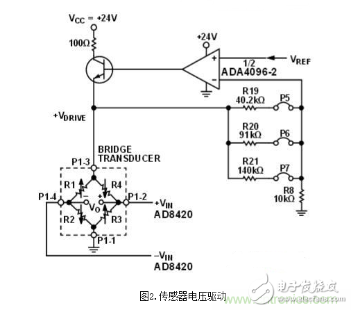
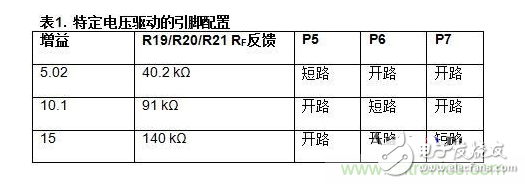
The gain is set by configuring the jumpers listed in Table 1.
The transfer function is calculated as follows:
Low-power, temperature-compensated bridge signal conditioner and driver circuit
Among them, RF can be 40.2kΩ, 91kΩ or 140kΩ, and R8=10kΩ.
NPN transistors are used to increase the current required to drive the bridge sensor. The feedback provided to the inverting input of the ADA4096-2 is such that the inverting input voltage is equal to the non-inverting input voltage, thereby ensuring that the voltage drive on the bridge circuit maintains a constant voltage.
Transistor Q1 is BJT with a maximum breakdown voltage of 80V and a power dissipation of 0.35W at 25°C. The collector maximum current is 500mA.
Instrumentation amplifierThe AD8420 rejects the common-mode voltage generated at the bridge and amplifies only the differential bridge voltage, as shown in Figure 3. The AD8420 has a rail-to-rail output voltage swing that is completely independent of the input common-mode voltage. This feature frees the AD8420 from the many limitations of the interaction between common-mode input and output voltages found in most traditional instrumentation amplifier architectures. The gain of this instrumentation amplifier is set to 1.
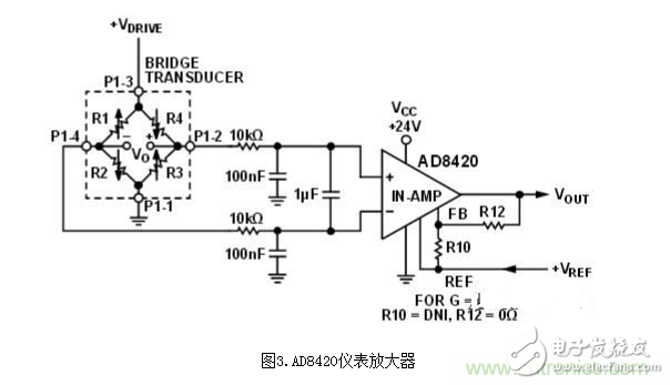
The input of the AD8420 has a differential mode noise filter (20kΩ/1μF/100nF) with a bandwidth of 7.6Hz and a common mode noise filter (10kΩ/100nF) with a bandwidth of 150Hz.
Traditional instrumentation amplifier architectures require a low-impedance source to drive the reference pin, and any impedance on the reference pin reduces the common-mode rejection ratio (CMRR) and gain accuracy. For the AD8420 architecture, the resistor on the reference pin has no effect on CMRR. The transfer function of the AD8420 is:
VOUT= G (VIN+- VIN-) + VREF
among them:
VREF= 1.05 V
G = 1 + (R12/R10)
The AD8420 differential input voltage is internally diode-limited to ±1V over the -40°C to +85°C temperature range. If the input voltage exceeds this limit, the internal diode begins to conduct and consume current. The current is internally limited to a value that guarantees the safety of the AD8420.
Reference buffer
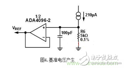
The 210μA excitation current generated by the AD7793 passes through a 5kΩ resistor, as shown in Figure 4. This will generate a 1.05V reference and then be buffered by the ADA4096-2. The output of the buffer drives the reference voltage source for the AD7793 and AD8420. This circuit is ratiometric, so the voltage variation on the 5kΩ resistor (caused by the 5% tolerance of the 210μA excitation current generated by the AD7793) is very small. The buffered reference voltage also drives the amplifier to set the voltage drive of the bridge sensor (see Figure 2).
ADC Channel 1 Configuration: Bridge Sensor
Channel 1 of the AD7793 measures the bridge sensor output of the AD8420. The external VREF (1.05V) is used as the reference voltage, so the input voltage range of the AD7793 is ±1.05V centered on the +1.05V common-mode voltage.
ADC channel 2 configuration: temperature sensor
The second channel of the AD7793 monitors the voltage developed across the resistance temperature detector (RTD), which is driven by a 210μA excitation current, as shown in Figure 5.
Although 100Ω platinum RTDs are very common, other resistors (200Ω, 500Ω, 1000Ω, etc.) and materials (nickel, copper, ferronickel) can be specified. This application uses a 100Ω DIN43, 760A RTD.
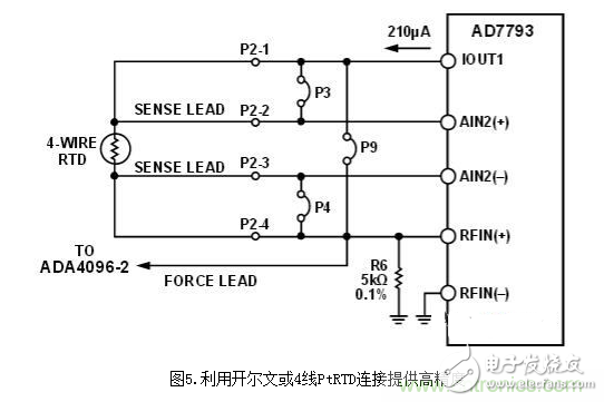
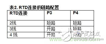
The 4-wire (Kelvin) connection shown in Figure 5 eliminates the RTD pin resistance effect. Note: With link P3 and link P4, you can also use 2-wire, 3-wire or 4-wire configurations, as shown in Table 2.
If temperature compensation is not required, the RTD can be bypassed using link P9.
Output coding
The output code of the input voltage on either channel is:
among them:
AIN=AIN(+)AIN(-)=AIN(+)VREF
Gain is the PGA gain setting, N=24.
Power supply voltage requirement
For the circuit to work properly, the supply voltage VCC must be greater than 6V to provide a minimum 5V drive for the bridge sensor.
System calibration
There are several ways to perform pressure sensor temperature calibration. This application uses a four-point calibration procedure. AN13-01 (active temperature compensation and calibration of MEMS pressure sensors at constant voltage) from SiliconMicrostructures, Inc. (Limbid, Calif.) provides a good reference for calibration procedures.
Test data and resultsSystem noise
All data capture operations are performed using the CN-0355 evaluation software.
To capture the evaluation board noise, two setup measurements were made. The first measurement is shown in Figure 6. The AD8420 input is short-circuited, thus measuring the peak-to-peak noise of the AD8420 and AD7793. After 1000 samples, the code distribution is approximately 100 codes, equivalent to 12.5μV peak-to-peak noise, or equivalent to 17.36 noise-free bits for a full-scale range of 2.1V.
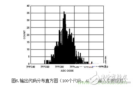
Figure 6. Output code distribution histogram (100 codes, shorted on the AD8420 input pin)
The second measurement was performed using a Honeywell NSCSANN600MGUNV pressure gauge sensor that was connected to the evaluation board. The pressure sensor mounted on the board is not amplified and compensated, and the voltage driver is set to 10.1V. This test effectively demonstrates the noise generated by the entire system, including sensor noise, as shown in Figure 7. 1000 samples were taken and the code distribution was approximately 120 codes, equivalent to 15μV peak-to-peak noise; or equivalent to 17.1 noise-free bits for a full-scale range of 2.1V.
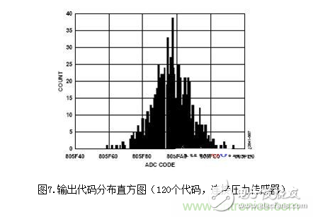
Figure 7. Output code distribution histogram (120 codes, connected to the pressure sensor)
System power consumption
Table 3 shows the total power consumption of the system, excluding the power consumption of the pressure sensor.
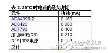
The Honeywell NSCSANN600MGUNV pressure sensor has an impedance of approximately 3kΩ, which increases the total power consumption shown in Table 3 by approximately 3.36mA.
Driving the RTD with a lower current (such as 10μA) while using a higher RTD resistance value (such as 1kΩ) can further reduce the power consumption of the system.
Error analysis of active componentsThe maximum error and root-slave (RSS) error caused by the active components AD8420 and ADA4096-2 in the system are shown in Table 4.
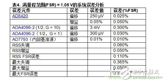
A reasonable approximation of the total error due to the resistance tolerance is assumed to be equal for each critical resistance contribution to the total error. The two key resistors are either R8 and R19, R20, R21. A 0.1% worst case resistor tolerance can result in a total resistance error of 0.2% of the maximum. If RSS error is assumed, the total RSS error is 0.1√2=0.14%.
The resistance error is added to the component error given in Table 4 to obtain the following results:
Offset error = 0.365% + 0.1400% = 0.555%
Gain error=0.050%+0.1400%=0.190%
Full scale error = 0.415% + 0.1400% = 0.555%
These errors use the assumption that the calculated resistance value is chosen, the tolerance is the only error, and the voltage drive of the sensor is set to a gain of 10.1.
The linearity error is tested at an input range of -500 mV to +500 mV using the settings shown in Figure 10. The total nonlinearity error is approximately 0.45%. Nonlinearity is primarily caused by the input transconductance (gm) level of the AD8420.
The total output error (%FSR) is obtained by dividing the difference between the measured output voltage and the ideal output voltage by the FSR of the output voltage and multiplying by 100. The calculation results are shown in Fig. 8.
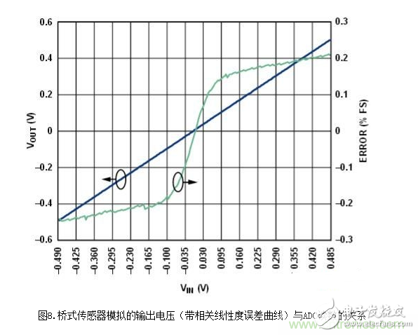
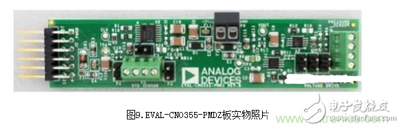
Figure 9 shows a physical photo of the EVAL-CN0355-PMDZ evaluation board. The complete documentation for this system is located in the CN-0355 Design Support Package.
Other suitable ADCs are the AD7792 and AD7785, which have the same combination of features as the AD7793. However, the AD7792 is a 16-bit ADC and the AD7785 is a 20-bit ADC.
The AD8237 is a micropower, zero-drift, true rail-to-rail instrumentation amplifier that can also be used in the low supply voltage version of this circuit configuration.
The AD8226 instrumentation amplifier is another option that achieves better linearity at higher power dissipation (approximately 525μA).
For low supply voltage range applications that require low noise and low offset voltages, the ADA4096-2 can be replaced with a dual AD8606. The dual AD8606 features very low offset voltage, low input voltage and current noise, and wide signal bandwidth. It uses ADI's patented DigiTrim technology to achieve outstanding accuracy without laser adjustment.
Circuit evaluation and testingThis circuit uses the EVAL-CN0355-PMDZ board, the EVAL-SDP-CB1Z System Demonstration Platform (SDP) evaluation board and the SDP-PMD-IB1Z (a PMOD adapter board for SDP). The SDP and SDP-PMD-IB1Z boards feature a 120-pin mating connector for quick setup and circuit performance evaluation. To evaluate the EVAL-CN0355-PMDZ board using the SDP-PMD-IB1Z and SDP, connect the EVAL-CN0355-PMDZ to the SDP-PMD via a standard right-angle pin header with a 100 mil spacing and 25 square mils. -IB1Z.
Equipment requirements
To evaluate and test the CN-0355 circuit, the following equipment is required:
Windows XP, Windows Vista (32-bit) or Windows 7 (32-bit) PC with USB port
EVAL-CN0355-PMDZ Circuit Evaluation Board
EVAL-SDP-CB1Z Circuit Evaluation Board
SDP-PMD-IB1Z adapter board
CN0355 evaluation software
6V wall power adapter or other power supply
Yokogawa GS200 precision voltage source
Agilent E3631A voltage source
start using
Put the CN-0355 evaluation software CD into your PC and load the evaluation software. Open my computer, find the drive containing the evaluation software CD, and open the Readme file. Follow the instructions in the Readme file to install and use the evaluation software.
Setting
The CN-0355 evaluation kit includes a CD containing self-installing software. The software is compatible with Windows XP (SP2) and Vista (32-bit and 64-bit). If the installation file does not run automatically, you can run the setup.exe file on the CD.
Please install the evaluation software first, then connect the evaluation board and SDP board to the USB port of the PC to ensure that the PC can correctly identify the evaluation system.
1. After the CD-ROM file is installed, power on the SDP-PMD-IB1Z evaluation board. Connect the SDP board (via connector A) to the SDP-PMD-IB1Z evaluation board with the supplied cable and connect to the PCUSB port for evaluation.
2. Connect the 12-pin right-angle male pin connector of the EVAL-CN0355-PMDZ to the 12-pin right-angle female pin connector of the SDP-PMD-IB1Z.
3. Connect the pressure sensor terminal and RTD sensor to the terminal socket of the EVAL-CN0355-PMDZ before running the program.
4. After connecting and turning on all peripherals and power, click the Run button on the graphical user interface. When the PC successfully detects the evaluation system, the evaluation software can be used to evaluate the EVAL-CN0355-PMDZ board.
Functional block diagram
The functional block diagram of the test setup is shown in Figure 10. This test setup must be connected as shown.
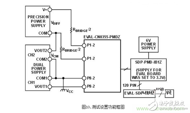
The Agilent E3631A and Yokogawa GS200 precision voltage sources were used to power the EV kit and simulate sensor output. The channel CH1 of the Agilent E3631A is set to 24V to serve as the VCC supply for the evaluation board, and the other channel CH2 is set to 5V to generate the common mode voltage. CH2 is connected in series with Yokogawa GS200, as shown in Figure 7. Yokogowa is connected to the input terminal of the EV kit via a 1.5kΩ series resistor that simulates the bridge impedance. Yokogawa simulates the sensor output by producing a ±500mV (at 25°C) differential input voltage at the input of the instrumentation amplifier.
The data from the EVAL-CN0355-PMDZ evaluation board was captured using the CN-0355 evaluation software to obtain the linearity error shown in Figure 8. The settings used are shown in Figure 10.
Fast Wireless Charger,Iphone Wireless Charger,Portable Wireless Charger,Best Wireless Phone Charger
wzc , https://www.dg-wzc.com