The TinySwitch-II series is designed for low-power, low-cost, high-efficiency switching power supplies up to 23W. For example, the miniaturized Switching Power Supply module in the IC card payment meter, the standby voltage of the mobile phone battery constant voltage / constant current charger, Power Adapter (Powersupplyadapter), microcomputer, color TV, laser printer, video recorder, camcorder, etc. Power Supply (Standbypowersupply), also suitable for ISDN and DSL network terminal equipment.
The optimized design of the switching power supply is facilitated by using TinySwitch-II. Due to the increased switching frequency to 132 kHz, the high frequency transformer allows the use of EE13 or EF12.6 miniaturized cores and achieves high power efficiency. TinySwitch-II has frequency jitter characteristics that allow EMI filtering with only one inductor (two small resistors with less than 3W output power or acceptable lower efficiency) and two capacitors. Even in short circuit conditions, high power rectifiers are not required.
1 Typical application of TinySwitch-II
1.1 2.5W constant current / constant voltage output mobile phone battery charger
The mobile phone battery charger circuit of 2.5W (5V, 0.5A) and AC wide range input consisting of TNY264 (IC1) is shown in Figure 1. RF is a blown resistor. The 85V~265V AC is rectified by VD1~VD4 bridge, and then the DC high voltage UI is obtained by the π-type filter composed of the inductor L1 and C1 and C2. R1 is the damping resistance of L1. Utilizing the frequency jitter characteristic of TNY264, it is possible to meet the international standard for suppressing conducted electromagnetic interference (EMI) between primary and secondary by using a simple filter and a low-cost safety capacitor C8 (Y capacitor). Even in the most unfavorable case where the output capacitive load is grounded, the EMI can be effectively suppressed by adding a shield to the high-frequency transformer. A clamp protection circuit consisting of diode VD6, capacitor C3 and resistor R2 limits the spike voltage applied to the drain when the power MOSFET is turned off within a safe range. When the output current IO is lower than 500 mA, the voltage control loop operates, and the current control loop does not function due to the transistor VT being turned off. At this time, the output voltage UO is set by the forward voltage drop (UF≈1V) of the LED in the optocoupler IC2 (LTV817) and the voltage regulator value of the Zener diode VDZ (UZ=3.9V), that is, UO=UF +UZ≈5V. Resistor R8 provides a bias current to the Zener diode, making the stable current IZ of VDZ close to typical values. After the secondary voltage is rectified and filtered by VD5, C5, L2 and C6, the +5V output voltage is obtained.
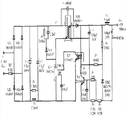
TinySwitch-II has a high switching frequency. During the reverse recovery process after the output rectifier VD5 is turned off, switching noise is generated, which easily damages the rectifier. Although the RC absorbing circuit formed by connecting the RC components at both ends of VD5 can suppress the switching noise, the effect is still not satisfactory, and the power loss is also caused in the resistor. The solution is to connect a magnetic bead in series with the secondary rectification filter.
Magnetic beads (Magneticbead) is an ultra-small amorphous alloy magnetic material that has been introduced in recent years. It is a two-material material with ferrite. The commercially available magnetic bead has a shape similar to that of a plastic-molded diode, and has a tubular shape, but is replaced by a magnetic material and has a small inductance made of a wire. Common magnetic beads have various dimensions such as Φ2.5×3 (mm), Φ2.5×8 (mm), and Φ3×5 (mm). For magnetic beads used in single-chip switching power supplies, the inductance is generally several to several tens of μH. The DC resistance of the magnetic beads is very small, generally 0.005 Ω to 0.01 Ω. Generally, the noise filter can only absorb the noise that has already occurred, which is a passive suppression type; the function of the magnetic beads is different, it can suppress the generation of switching noise, and therefore belongs to the active suppression type, which is the fundamental difference between the two. Magnetic beads can be widely used in high frequency switching power supplies, video recorders, electronic measuring instruments, and various circuits where noise is very strict. The filter inductor L2 in Figure 1 uses a 3.3μH magnetic bead to filter out the switching noise generated by VD5 during reverse recovery.
The current control loop is composed of a transistor VT, a current detecting resistor R4, and an optocoupler IC2. When the output current IO is close to 500mA, the emitter voltage UBE of the transistor VT also rises due to the voltage drop across R4, and the VT enters the amplification region. At this time, the current control loop starts to function and the output is constant current. characteristic. Even if a short-circuit fault occurs at the output, IO↑, UO→0V, because the total voltage drop across resistors R6 and R4 is about 1.2V, the normal operation of the LED in the VT and optocoupler can be maintained. R3 is the base current limiting resistor.
1.2 15W PC standby power circuit
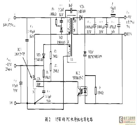
A PC standby power supply circuit with an output power of 15W is shown in Figure 2. The power supply provides two outputs: the main output is +5V, 3A; the auxiliary output is +12V, 20mA. The total output power is 15.24W and the power efficiency is higher than 78%. Two integrated circuits are used in the circuit: TNY267P miniature monolithic switching power supply (IC1) and SFH615-2 linear optical coupler (IC2). The DC input voltage is 140V to 375V, which corresponds to the case where the AC input voltage is 230V ± 15% or 110/115V double voltage input. The undervoltage detection, auto-restart and high-frequency switching characteristics of the TNY267P allow the use of a smaller, lower-priced EE22 high-frequency transformer core. The TNY267P is available in a DIP-8 package that filters out glitches on the output voltage waveform when auto-restarting due to slow discharge of the output filter capacitor. When the input voltage is lower than the undervoltage, the TNY267P automatically shuts down for protection; it only works when the input voltage is above the undervoltage threshold. R2 and R3 are undervoltage threshold setting resistors. When the total resistance of the two is 4MΩ, the undervoltage threshold is set to 200V DC, and the rectified DC high voltage UI must be higher than 200V to turn on the power. Once the power is turned on, it will continue to work until the UI drops to 140V. This hysteretic shutdown feature provides the required hold-up time for the standby power supply.
The auxiliary winding on the primary side is rectified and filtered by VD2 and C2, and the output voltage of +12V is obtained, and the TNY267P is supplied with power through R4. The TNY267P internal drain-driven current source also stops charging the external bypass capacitor during normal operation to reduce static losses. When R4=10kΩ is selected, 640μA current can be supplied to the bypass terminal, which is slightly higher than the loss current of TNY267P. The excess will be clamped by the internal Zener diode to the safe voltage of 6.3V.
The secondary output is rectified and filtered by VD3, C6 and C7. L and C8 form a post-stage filter, which is mainly used to filter out switching noise. When the output is shorted, the auto-restart circuit limits the increase in output current and filters out the overshoot voltage to VD3. The 5V output is detected by the optocoupler IC2 (SFH615-2) and the Zener diode VDZ, and the R5 supplies a bias current to the Zener diode.
2 circuit design points
2.1 Precautions for use
(1) The minimum value UImin of the DC input voltage UI can be designed as 90V. When inputting a wide range voltage (85V ~ 265V), the capacity of the input stage filter capacitor C1 can be selected according to the proportional coefficient of 3μF / W; for example, when the output power PO = 10W, C1 = 30μF. For AC 230V ± 15% fixed voltage input, the scaling factor can be 1μF / W.
(2) In order to reduce the loss and improve the power efficiency, the secondary rectifier should use Schottky Barrier Diode (SBD), referred to as Schottky diode. The tube has the advantages of low forward voltage (UF ≈ 0.4V), low power loss, short reverse recovery time (trr can be as small as several ns), and is suitable for low voltage, high current rectification or freewheeling.
(3) Selecting a TinySwitch-II chip with a large output power helps to improve power efficiency. For example, in the circuit shown in Figure 2, the lower limit of the power efficiency when selecting TNY267 is 78%; if TNY266 and TNY264 are used, it is reduced to 76% and 74%.
(4) In a specific application, the maximum output power of TinySwitch-II depends on the thermal environment (including ambient temperature, heat dissipation conditions, ventilation conditions, and whether the power supply is sealed or open), the size of the high-frequency transformer core, and the work. The design of the mode (continuous mode or discontinuous mode), the required power, the minimum value of the input voltage, the capacity of the input stage filter capacitor, and the forward voltage drop of the output rectifier vary.
(5) TinySwitch-II can filter out the audio noise generated by high-frequency transformers. Allows the use of a common structure of the varnish transformer, the core can also be glued without glue. When the switching power supply generates audio interference due to the reduction of the load, TinySwitch II reduces the audible noise by discontinuously reducing the limit current value.
(6) The LTV817 linear optical coupler in Figure 1 can be replaced by PC817 or PC817A. Their technical parameters are basically the same, the current transmission ratio CTR = 80% ~ 160%, the reverse breakdown voltage U (BR) CEO ≥ 35V.
(7) In the circuit shown in Figure 2, if the standby power supply selects the TNY266P chip, the output power is reduced to 10W. At this time, the EE16 type high frequency transformer core can be selected, and the filter capacitor C7 can also be removed.
2.2 Printed board design points
The printed circuit board component layout of the TinySwitch-II chip is shown in Figure 3. The undervoltage protection resistor is not used here. The following must be noted when designing a printed board:
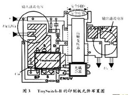
(1) The copper-clad plate under the TinySwitch-II not only acts as a source grounding point but also acts as a heat sink. The area of ​​the shaded area in Figure 3 should be large enough to ensure good heat dissipation of the TinySwitch-II and secondary rectifiers, resulting in a junction temperature of less than 100 °C.
(2) The bypass capacitor CBP and the input filter capacitor C1 must be connected to the source terminal by a single-point grounding method. The primary circuit connecting C1, high frequency transformer and TinySwitch-II should be as short as possible.
(3) The primary clamp circuit is used to limit the peak voltage on the drain at turn-off. It can be implemented with R, C, and VD clamp circuits. The drain voltage can also be clamped with a 200V Zener diode or a transient voltage suppressor (TVS). In any case, the distance between the clamp components and the high-frequency transformer and TinySwitch-II should be the shortest.
(4) If an undervoltage detection resistor is used, the resistor should be placed as close as possible to the EN/UV terminal to reduce induced noise. It is also necessary to consider the withstand voltage values ​​of the undervoltage detecting resistors R2 and R3. When selecting the resistance of (1/4)W, it can generally withstand 200V voltage (refer to continuous pressurization, the same below); for the resistance of (1/2)W, the withstand voltage is 400V.
(5) The safety capacitor (Y capacitor) should be installed directly between the positive and negative ground (return) of the primary filter capacitor to minimize electromagnetic interference and common mode surge voltage.
(6) The distance between the optocoupler and the EN/UV terminal of the TinySwitch-II should be the shortest to reduce noise coupling. The distance from the EN/UV pin to the optocoupler should be less than 12.7 mm and the distance to the drain should be greater than 5.1 mm.
(7) In order to improve the voltage regulation performance, the loop connected to the secondary winding, the secondary rectifier, and the secondary filter capacitor should be as short as possible. The pad area of ​​the secondary rectifier must be large enough to ensure that the heat of the rectifier diode is dissipated in a timely manner in the event of an output short circuit.
Edit: Nizi
Yidashun supplies Wall Socket and Extension Socket for different countries.
Power outlet is US, EU, UK, AUS, CN, Japan, and Korea optional. Standard groundin
power Socket is with switch control and led indicator, and the switch contact ismade of high quality silver alloy material, which has a good performance against
electric arc and melt weld. The on-off operations exceed 40000 times.
Besides, the socket is made of phosphor bronze, which has the character of good electrical conductivity and lasting elasticity. The USB ports on the electrical outlet are 5V2.1A output which are compatible with APPLE ipad (all models), iphone, Android phones and tablet, cell phones, gaming systems, digital cameras, GPS devices and all USB devices.


Wall Socket
Wall Socket,Wall Power Socket,Smart Wall Socket,Wall Plug Socket
Shenzhen Yidashun Technology Co., Ltd. , https://www.ydsadapter.com