The first chapter introduces the AM824-Core development kit. This article covers sections 1.1 (LPC824 microcontroller) and 1.2 (LPC84x microcontroller).
This chapter guides:
With the rapid development of Internet of Things (IoT) technology, the capabilities of microcontroller units (MCUs) have significantly advanced. The distinction between MCUs and microprocessors is becoming less clear, with MCUs increasingly integrating into embedded systems. AMetal simplifies this process by abstracting the underlying complexity, allowing developers to focus on basic MCU functionalities without worrying about intricate details.
1.1 LPC824 Microcontroller
>>> 1.1.1 Features
System:
- ARM Cortex-M0+ embedded processor with a built-in nested interrupt vector controller (NVIC), system tick timer, and runtime frequency up to 30 MHz;
- Supports Serial Wire Debug (SWD) mode and JTAG Boundary Scan (BSDL) mode.
On-chip memory:
- Up to 32KB Flash and 8KB SRAM with 64-byte page write/erase capability.
Digital peripherals:
- Up to 32 general-purpose I/O pins with configurable pull-up/pull-down, open-drain mode, input inverter, and filter;
- GPIO directional control supports independent set, clear, and flip operations;
- 4 pins with 20mA output drive, 2 open-drain pins with 20mA sink drive;
- GPIO interrupt generation with 8 inputs supporting Boolean pattern matching;
- Switch matrix for flexible I/O configuration;
- CRC engine with 18 channels and 9 trigger inputs.
Timers:
- SCTimer/PWM for timing and PWM applications with capture and match functions;
- Quad Channel Multi Rate Timer (MRT) for repeatable interrupts at 4 programmable rates;
- Self-wake timer (WKT) using internal or external clock sources;
- Window Watchdog Timer (WWDT).
Analog peripherals:
- 12-bit ADC with up to 12 channels, 1.2 Msamples/s sampling rate, and support for two independent conversion sequences;
- Comparator with 4 input pins and internal/external reference.
Serial interfaces:
- 3 USART interfaces with switch matrix pin assignment and shared fractional baud rate generator;
- 2 SPI controllers with switch matrix pin assignment;
- 4 I2C bus interfaces supporting high-speed mode, 1 Mbps, and 400 kbps standard modes.
Clock generation:
- 12MHz internal RC oscillator with ±1.5% accuracy;
- Crystal oscillator from 1MHz to 25MHz;
- Programmable watchdog oscillator (9.4kHz–2.3MHz);
- 10kHz low-power oscillator for WKT;
- PLL for CPU frequency generation without high-frequency crystals;
- Clock output with divider for all internal clocks.
Power control:
- Integrated PMU for power optimization;
- Low-power modes: sleep, deep sleep, power down, and deep power down;
- Wake-up from USART, SPI, and I2C in deep sleep/power down;
- Self-wake via timer in deep power down;
- POR and BOD for reset and brownout detection.
Single power supply: 1.8V – 3.6V; operating temperature: -40°C – +105°C.
>>> 1.1.2 Overview
The LPC824 series microcontrollers (MCUs), as shown in Figure 1.1, offer a rich set of on-chip peripherals including a switch matrix, state-configurable timers, multi-rate timers, window watchdog timers, and DMA. Analog peripherals include a 12-bit high-speed ADC and an analog comparator. The device also features three UARTs, two SPIs, and four I2C interfaces. A 12MHz internal RC oscillator serves as the system clock source.
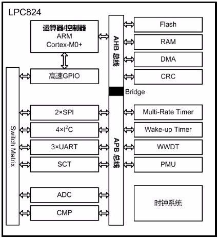
Figure 1.1: LPC824 Functional Block Diagram
The LPC824 series is known for its ultra-low power consumption (90μA/MHz), with four power-saving modes that allow users to choose based on application needs. The lowest power mode consumes less than 1μA. While these concepts may seem complex at first, they are similar to how computers work—complex under the hood but easy to use for programming and web browsing.
The LPC812/824 belongs to the LPC800 series. The LPC824 is an enhanced version of the LPC812, offering more peripheral resources and better adaptability to various applications. Due to consistent register configurations across peripherals, software design remains compatible, reducing platform development difficulty and enabling flexible selection based on requirements. See Table 1.1 for details.
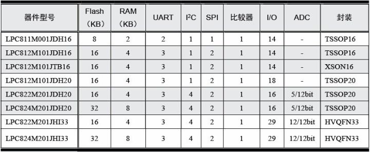
Table 1.1: LPC800 Series MCU Selection Table
The LPC824 series is available in TSSOP20 and HVQFN33 packages, as shown in Figure 1.2.
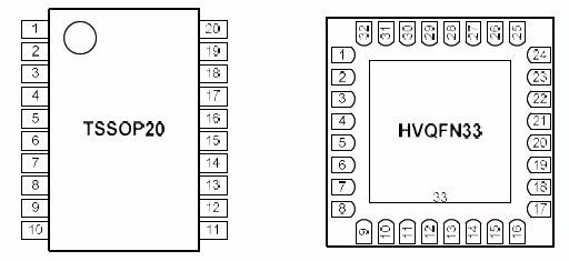
Figure 1.2: LPC824 Package Schematic
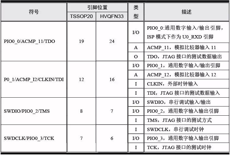
The pin descriptions and main functions of the LPC824 series are detailed in Table 1.2.
1.2 LPC84x Microcontroller
>>> 1.2.1 Features
System:
- ARM Cortex-M0+ processor with runtime frequency up to 30 MHz, single-cycle multiplication, and fast single-cycle I/O;
- Built-in NVIC;
- System tick timer;
- AHB bus matrix;
- Support for SWD and JTAG;
- Micro Tracking Buffer (MTB).
Memory:
- Up to 64KB Flash with 64-byte page write/erase;
- FAIM memory for power-up behavior configuration;
- CRP (Code Read Protection);
- Up to 16KB SRAM, including 2 x 8KB contiguous SRAMs, one used by MTB;
- Support for bit-band operations for atomic bit manipulation.
ROM API Support:
- Bootloader;
- IAP (In-Application Programming);
- ISP (In-System Programming) via USART, SPI, or I2C;
- Integer division API interface.
Digital peripherals:
- Up to 32 general-purpose I/O pins with configurable pull-up/pull-down, open-drain mode, input inverter, and filter;
- 4 pins with 20mA output drive;
- 2 open-drain pins with 20mA sink drive;
- GPIO interrupt with 8 inputs and Boolean pattern matching;
- Switch matrix for flexible I/O configuration;
- CRC engine;
- 25-channel DMA with 13 trigger inputs;
- Capacitive touch screen interface.
Timers:
- SCTimer/PWM with 8 match/capture, 8 events, 8 states;
- 1 general-purpose timer with 4 matched outputs, 3 input captures, PWM, and DMA support;
- Quad Channel MRT for 4 programmable fixed-rate interrupts;
- Self-wake timer (WKT) using internal or external clock;
- Window Watchdog Timer (WWDT).
Analog peripherals:
- 12-bit ADC with 12 channels, 1.2 Msamples/s, and two independent conversion sequences;
- Comparator with 4 input pins and internal/external reference;
- Two 10-bit DACs.
Serial interfaces:
- 5 USART interfaces with switch matrix and shared fractional baud rate generator;
- 2 SPI controllers with switch matrix;
- 4 I2C interfaces supporting high-speed mode, 1 Mbps, and 400 kbps standard mode.
Clock generation:
- Free running oscillator (FRO) with ±1% accuracy, providing 18MHz, 24MHz, or 30MHz;
- Low-power startup at 3MHz using FAIM;
- Crystal oscillator from 1MHz to 25MHz;
- Low-power oscillator for watchdog;
- Programmable watchdog oscillator (9.4kHz–2.3MHz);
- PLL for CPU frequency generation;
- Clock output with divider for all internal clocks.
Power control:
- Low power consumption: 90μA/MHz;
- Integrated PMU for power optimization;
- Low-power modes: sleep, deep sleep, power down, and deep power down;
- Wake-up from USART, SPI, and I2C in deep sleep/power down;
- Self-wake via timer in deep power down;
- POR and BOD for reset and brownout detection.
Single power supply: 1.8V – 3.6V; operating temperature: -40°C – +105°C;
Available in LQFP64, LQFP48, HVQFN48, and HVQFN33 packages.
>>> 1.2.2 Overview
The LPC84x family of microcontrollers (MCUs), as shown in Figure 1.3, includes a wide range of on-chip peripherals such as switch matrix, state-configurable timers, multi-rate timers, window watchdog timers, and DMA. Analog peripherals include a 12-bit high-speed ADC and two 10-bit DACs, along with five UARTs, two SPIs, and four I2C interfaces. A free-running oscillator is integrated into the chip as the system clock source.
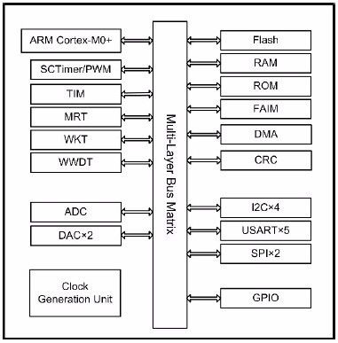
Figure 1.3: LPC84x Functional Block Diagram
The LPC84x series is also known for its ultra-low power consumption (90μA/MHz), with four low-power modes that allow users to select the best option based on their application needs. The lowest power mode consumes less than 1μA. Though these features may seem complex at first, they are designed to simplify development and make the MCU user-friendly, much like how your computer works—complex internally, yet simple to use for daily tasks.
The LPC84x series comes in four different package options, making it suitable for a wide range of applications. See Table 1.3 for details.
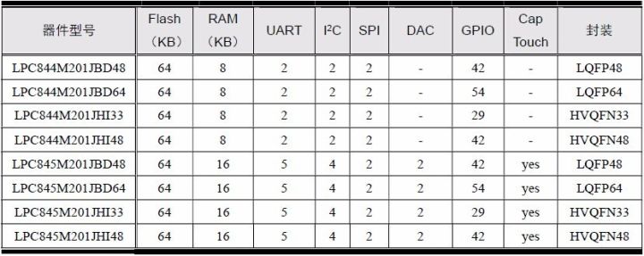
Table 1.3: LPC84x Series MCU Selection Table
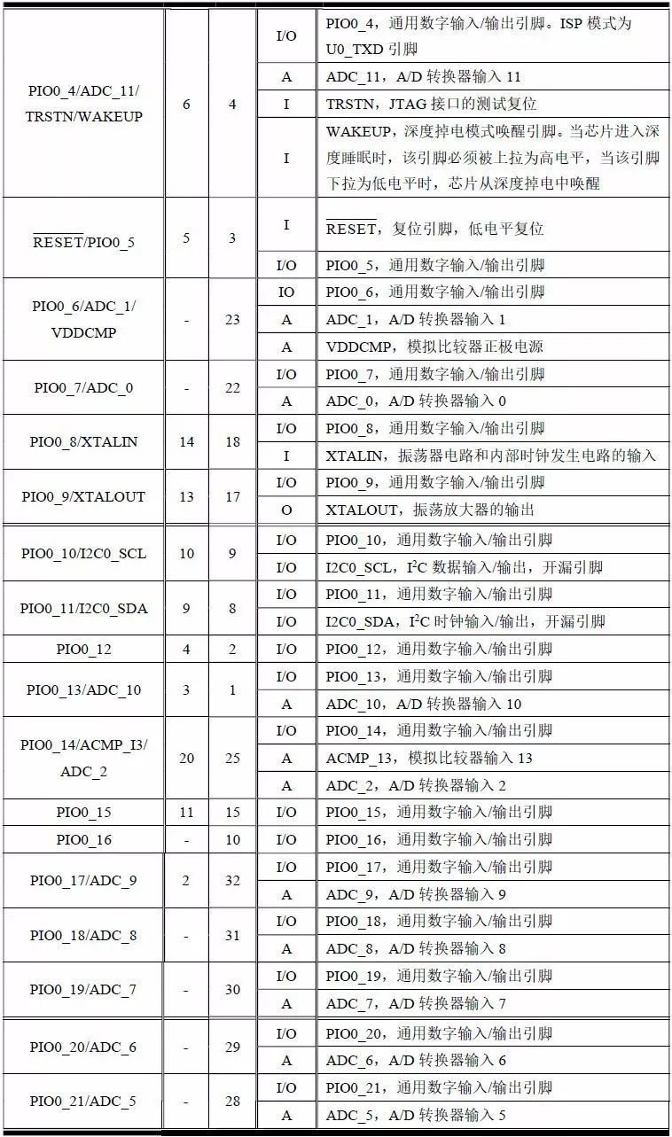
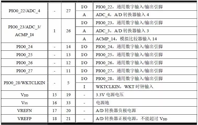
The pin descriptions and main functions of the LPC84x series are listed in Table 1.4.
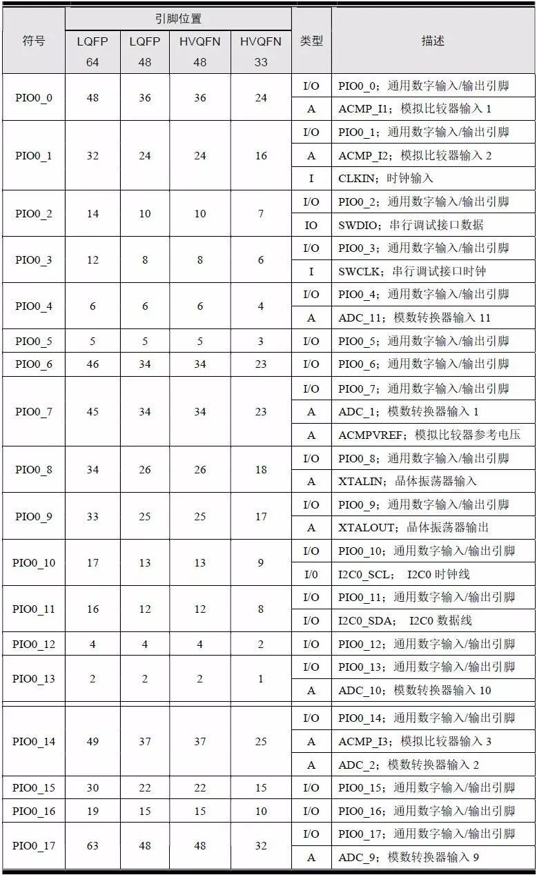
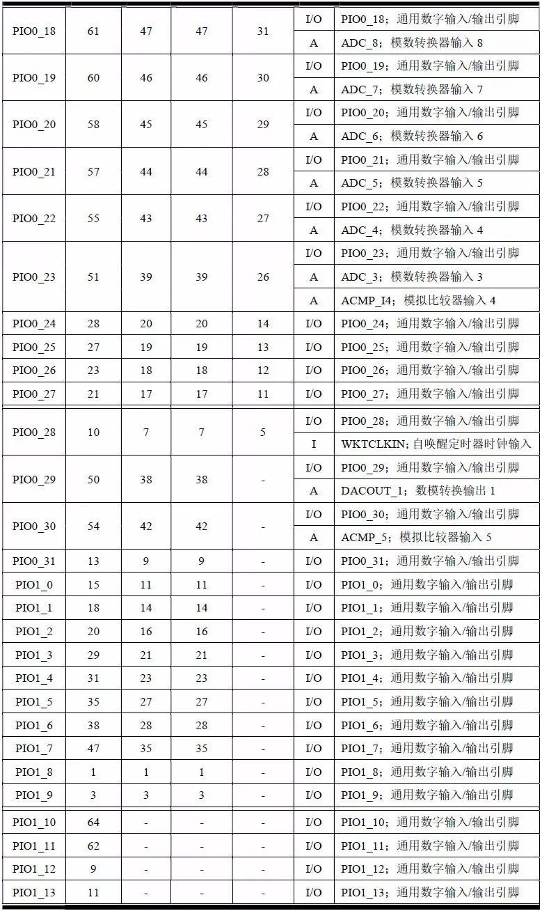
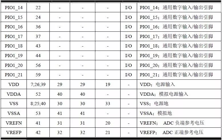
Table 1.4: LPC84x Pin Description
Harvester Drive Wheel,Belt Drive Pulley,Power Take-Off Shaft,Agricultural Gearbox
Changzhou Youeryou Trading Co., Ltd. , https://www.farmpartssupplier.com