Use thermal analysis to predict IC transient effects and avoid overheating
This paper proposes a method to predict the thermal performance of IC. This information is particularly useful for PMICs (power management ICs) used in automobiles and other high-temperature environments. By analyzing the thermal performance, we designed a mathematical model to simulate the transient temperature inside the chip. We introduced physical laws about thermal performance and used them to evaluate the IC's heating model. Based on these analyses, we propose an equivalent passive RC network used to simulate the IC transient thermal performance model. To illustrate the application of this analysis, we designed an RC network for LED drivers (MAX16828). Finally, it summarizes the use and effectiveness of this method, and puts forward ways to accelerate the construction of RC models.
Designers often need to understand the thermal performance of ICs, especially PMIC (Power Management IC) in automotive applications. When the actual IC works in a high-temperature environment (for example, + 125 ° C), will it trigger a thermal shutdown circuit or exceed the safe operating temperature range of the product? Without a clear analytical method, we cannot answer this question exactly. Therefore, when defining a new IC, we need a way to predict thermal shutdown or excessive die temperature based on complex internal functions.
In the DC operating mode, the parameters provided by the data can often be used to determine the junction temperature, such as θJA (thermal resistance) and θJC (junction temperature thermal characteristics) 1. However, in order to predict how high the junction temperature peaks outside the DC mode (for example, a power MOSFET driven by a PWM signal to control an LED or a switching regulator), it is necessary to understand the transient thermal characteristic data. Although this data is very useful, it is usually not provided in the data sheet. You may also need to know how long the chip can operate without failure at a given power dissipation level. This question is also difficult to answer.
This article solves the problem of using power consumption and ambient temperature to predict the junction temperature of the chip, which is a function of time. This article first introduces the physical laws on which the analytical methods are based. Then the IC system is defined as a complex layered thermal body model for discussion. Then theoretical analysis of the thermal body model is carried out, and the expression of transient thermal performance is obtained. This paper proposes an equivalent RC passive network based on these formulas, which is used to represent the thermal characteristics of the IC. Finally, in order to prove the effectiveness and accuracy of this analysis method, the article gives the experimental results of the MAX16828 high voltage linear HB LED (high brightness LED) driver circuit with PWM dimming function.
Law of thermodynamics
For any object, the relationship between temperature and time can be obtained by the following two basic laws.
Newton's law of cooling:
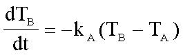 (Formula 1)
among them:
TB is the object temperature, TA is the ambient temperature. kA is a proportional constant (> 0).
t is time.
According to the law of conservation of energy:
mcΔT = energy = PΔt
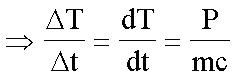 (Formula 2)
among them:
P is the constant power generated by or transferred to the heat source.
m is the mass of the heating element.
c is the heat capacity of a specific object.
Combining these two laws, we get:
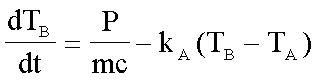 (Formula 3)
IC data sheets usually list the thermal characteristics of the package, such as θJA. We can use this data to analyze the steady-state thermal balance of the package to check whether Equation 3:
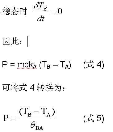
among them:
θBA is thermal resistance-object to environment.
TB is the temperature inside the package.
TA is the external ambient temperature.
Therefore: 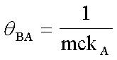 (Formula 6)
Define the chip as a thermal system
It is important to define the system clearly, because the thermal analysis results depend on this definition. From the cross-section of the chip mounted on the PCB (Figure 1), we can see that there are at least three different materials from the die to the ambient channel: the die itself, the epoxy mold, and the package. Depending on the location of the main heat source, the thermal model is based on one of two heat flow patterns: from the external heat source to the die (when the external heat source is the main heat source) and from the die to the external environment (when the die is the main heat source). We discuss these two models separately.
Heat flow from external heat source to chip
Consider the system shown in Figure 2, which shows a schematic diagram of a uniform object obtaining energy (heat) from a power source and releasing energy to the external environment.
The heat reaches the inner die through the encapsulation and mold compound. Therefore, the system also simulates the transient thermal characteristics of the chip when the heat source is outside the package. Since the die has many metals, the package thermal resistance is usually much higher than the die itself. Therefore, the die temperature changes with the package temperature, with almost no lag, making the chip look like a whole. We can use Equation 3 to define this overall system. Solving for TB, we get:
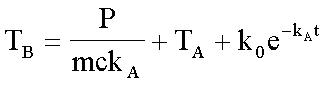 (Equation 7)
Among them, k0 is the integral constant, which is obtained by solving the initial conditions. Generally speaking, this formula is very useful for defining the transient thermal characteristics of the chip when the heat source is outside the chip.
This model can be explained by an example. To determine the transient thermal characteristics of the chip, its initial temperature is TI, t = 0, TB = TI:
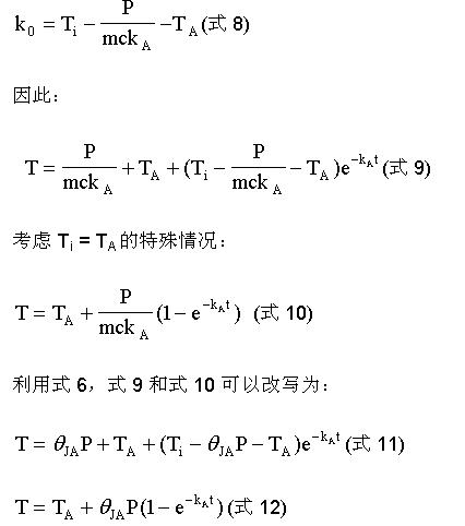
Equation 11 and Equation 12 are very useful for predicting chip temperature (whether package or die) when the heat source is outside the package. A special case of a heat source is a large current MOSFET that needs to dissipate a large amount of heat.
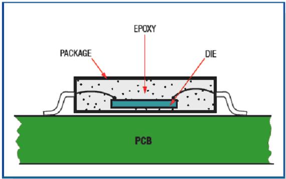
Figure 1. Cross-section of a chip mounted on a PCB, showing the material level between the die and the environment. 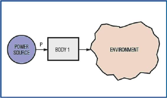
Figure 2. This thermal model illustrates the flow of heat from an external power source to the chip (component 1) and then back to the environment.
Knowing kA and θJA, the temperature at different times can be calculated. Or, if P is a composite function of time, you can use the above formula as a time simulation to evaluate the temperature, and use MATLAB® software to program the function of temperature as a function of time. θJA is provided by data. However, if a certain configuration condition is different from the provisions of the JEDEC standard, calculation using the published θJA value will cause an error. Section 51-3 of the JEDED standard states: "It is worth emphasizing that the values ​​obtained with these test boards cannot be used to directly predict the performance of any specific application system, but can only be used for comparison between packages" 2. Therefore, in order to estimate the temperature correctly, the θJA value should be measured for the prototype development board, or directly estimated according to the following instructions.
Heat flow from die to environment
Consider the three-body system shown in Figure 3 (similar to a chip), which generates heat at the die and dissipates the heat to the external environment through epoxy and packaging. Component 1 is a die, component 2 is epoxy resin, and component 3 is a chip package.
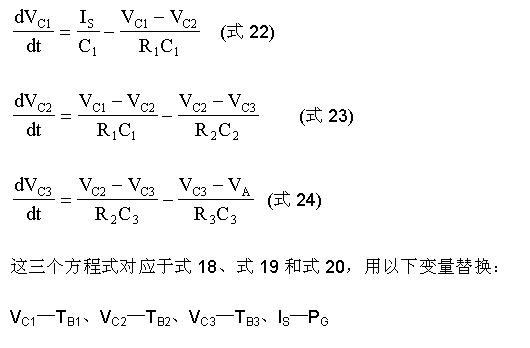
In order to solve θJA in this system, we must define formulas for three objects.
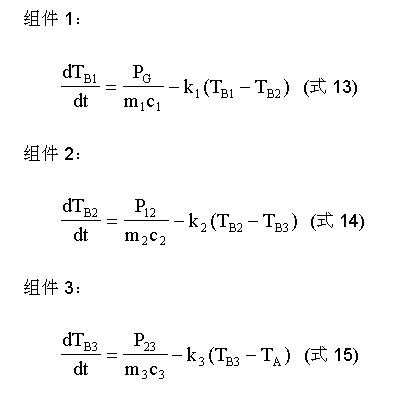
among them:
TB1, TB2, and TB3 are the instantaneous temperatures of modules 1, 2, and 3, respectively; P12 is the power conducted from module 1 to module 2 in the form of heat; P23 is the power conducted from module 2 to module 3 in the form of heat; PG is the module 1 Power directly generated, or power conducted directly to component 1. The power generated by the die (PG) minus the power absorbed by the die yields:
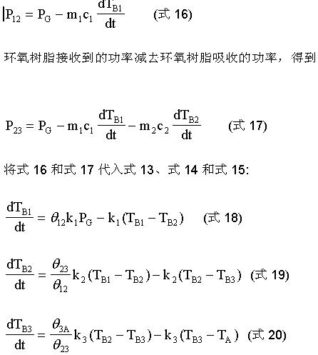
Solving the three-body system from Equation 18, Equation 19, and Equation 20 is more complicated, but the Laplace transform can simplify the calculation. The solution formula is:
 (Equation 21)
among them:
θ12 is the thermal resistance of component 1 to component 2; θ23 is the thermal resistance of component 2 to component 3; θ3A is the thermal resistance of component 3 to environment; T1, T2 and T3 are the integral constants; m1, m2 and m3 are k1 and k2 And k3 functions.
When the die generates power, Equation 21 can predict the die temperature in a very accurate way. However, when using this formula, we must know all the integration constants and m1, m2, and m3, which are complex functions and difficult to solve. To avoid this difficult operation, we use a tool to solve different equations: SPICE.
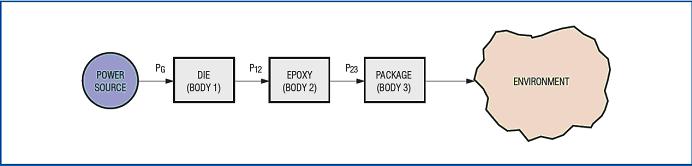
Figure 3. Comparison of the three-body model with the model shown in Figure 2. At this time, the heat flow generated by the die is more complicated.
Differential equation of transient thermal characteristics of RC network model
Now, we propose a similar differential equation for circuit modeling. We simulate the circuit and obtain temperature readings through the simulation. Differential equations 18, 19, and 20 can be simulated by a simple RC network (Figure 4) representing the power generated by the die.
In Figure 4, the initial voltage of the capacitor represents the temperature of the die (C1), epoxy (C2), and package (C3), respectively. VA represents the ambient temperature and IS (current flowing into capacitor C1) represents the power generated by the die. The difference equation representing the capacitor voltage is:
The capacitor voltage is directly related to the temperature of the die, epoxy, and package. Any SPICE toolkit can easily simulate RC circuits. If the appropriate parameters of R1, R2, R3, C1, C2, and C3 of the specific chip model are known, the circuit can be simulated and the die temperature can be directly read in the form of capacitor C1 voltage.
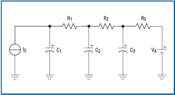
Figure 4. This RC network is used to simulate the transient thermal characteristics of the chip when heat is generated internally.
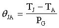
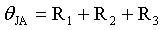
Now, we can determine the passive component values ​​for specific chips (R1, R2, R3, C1, C2, and C3). By measuring the final steady-state temperature of the die, the thermal resistance (θJA) of the system is obtained using Equation 5 (rewritten below as Equation 25):
 (Equation 25)
Among them: TJ is the steady-state junction temperature of the die; TA is the ambient temperature; PG is the dissipated power of the die.
Working under the same power dissipation (PG) as Equation 25, starting from time 0, the die temperature measured at different times can constitute a set of data that reflects the instantaneous temperature change of the die. Then, according to the following constraints, curve fitting is performed on the measured data to determine the values ​​of R1, R2, R3, C1, C2, and C3.
 (Equation 26)
Measuring die temperature
There are several methods for measuring the die temperature of integrated circuits3. Here, we will use the ESD diode forward voltage drop measurement method to determine the chip temperature, because this method is simple and does not introduce large errors. However, in order to ensure that the measurement error is within an acceptable range, it is necessary to carefully select the measurement technology of the die temperature for the specific chip. Practice has proved that it is critical to follow the following principles3.
1. Make sure that the ESD diode selected for measurement does not have a large parasitic resistance, nor will a large current flow, so as not to cause deviation in the diode voltage drop reading. It is best to discuss with the IC manufacturer to determine the maximum estimate of the internal wire bond and metal resistance.
2. Also make sure that the ESD diode is close to the chip heat source or in an area where the die temperature is actually considered. This configuration can better estimate the temperature and obtain more accurate results.
3. If the on-resistance of the FET is selected to estimate the temperature indication, make sure that the FET is fully turned on at the test temperature and is at the minimum voltage drop
When the forward voltage drop of the ESD diode is used for measurement, the diode on the chip needs to be forward biased to measure its voltage. Most chips can easily do this by connecting the ESD diode between the pin and the supply voltage. Because the measured data is the diode voltage drop, the relationship between diode voltage and temperature must also be considered.
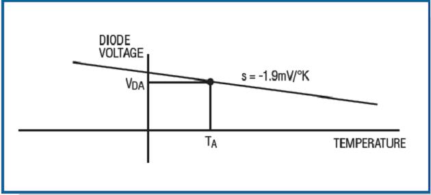
Figure 5. Diode forward voltage drop versus temperature under fixed current bias.
The diode voltage drops with a nearly constant slope, and the deviation is negligible. If you draw a curve that changes with temperature, you can get a result similar to Figure 5. In Figure 5, TA is the ambient temperature and VDA is the diode voltage at the ambient temperature. From this, we get a point and slope on the curve. The slope can be obtained by measuring the diode voltage at different temperature points in the temperature controlled furnace. Or use a common value: 2mV / ° K, which is effective in various diode current ranges with a small error of 4. These values ​​are also applicable to other chips, but for accuracy, it is best to measure the slope corresponding to the diode bias current. So far, you can use the diode voltage to represent any temperature:
In order to properly use the RC network for curve fitting of measured diode voltage transient data, we only need to set the amplitude of the current source to: IS = sPG (Eq. 33)
Since s <0, Equation 33 can be implemented by reversing the current source and setting its amplitude to | sPG |.
Experimental determination and verification of RC network
We can use the equations and linear LED drivers (such as the MAX16828 / MAX16815) obtained above to verify the practical application of the RC simulation model. These chips work at voltages up to 40V and require almost no external components. The MAX16828 can power a string of LEDs with a maximum current of 200mA (Figure 6). The MAX16815 is pin compatible with MAX16828 and has similar functions, but the maximum output current can reach 100mA instead of 200mA. Both LED drivers are suitable for automotive applications, for example, for side lights, car tail lights, backlights and indicator lights. If the internal MOSFET needs to withstand a large current and has a large voltage drop, the MAX16828 will need to dissipate considerable heat (this happens when the forward voltage of the LED string is low). The voltage across RSENSE is regulated at 200mV ± 3.5%. This resistor is used to set the LED current. The chip's DIM input provides a wide range of PWM dimming for the LED because it can withstand high voltages and can be directly connected to the IN pin. To directly display the die temperature, we measured the forward bias voltage of the internal ESD diode connected between the DIM and IN pins. The diode is biased at approximately 100μA, and its forward voltage change rate is 2mV / ° K (this can be verified by heating the device with a temperature-controlled furnace). The experimental setup is shown in Figure 7. The 5V power supply and 56kΩ resistor provide 100μA bias current, which provides forward bias for the ESD diode. The driver is set to provide an output current of 200mA to the LED.

Figure 6. Typical application circuit of the MAX16815 / MAX16828 HBLED driver. 
Figure 7. The test setup shown in the figure uses an on-chip ESD diode to measure the instantaneous temperature of the die. * EP means exposed pad.
In this state, the component carries a lot of current, and the ESD diode measurement is in the measurement path. Therefore, due to the influence of the welding wire and the internal metal resistance, a certain error will occur. Based on the internal layout and the length of the welding line, the worst-case parasitic resistance is estimated to be 50mΩ. At 200mA, this parasitic resistance will produce an error of approximately ± 10mV (maximum) on the diode reading, and the corresponding temperature measurement accuracy error is greater than ± 5 ° C. In addition, the die ESD diode is placed close to the on-chip power MOSFET and thermal protection circuit. This configuration allows the diode to more accurately represent the temperature in that area.
System definition 1
The next section describes how to use the test device to collect the diode voltage representing the instantaneous thermal characteristics, which is used in the above system definition equations of Equation 7 and Equation 21. In order to calculate kA and θJA (substitute into formula 11), a heat gun is used to heat the chip. Because we don't want to generate heat inside the chip, power off the chip. Heating elements with a hot air gun will increase the temperature of the package and die. An oscilloscope can be used to measure the voltage of the diode to monitor the temperature change of the die (Figure 8).
When the chip is heated, the diode voltage drops rapidly according to the exponential law, which is consistent with the prediction result of the formula. When approaching the middle of the curve, turn off the heat gun to allow the package and die to cool. The diode voltage rises again according to the exponential law. We do not know exactly how much heat is transferred from the heat gun to the chip. Therefore, in order to eliminate this unknown number, we first adjust Equation 28 to fit only the rising part (cooling) of the curve (Figure 8). This curve fitting allows us to estimate the optimal value of kA. During cooling, no thermal power is transferred to the package, the package is only cooled, P = 0. Therefore, Equation 28 can be simplified to:
![]() (Equation 34)
(Equation 34)
We know the values ​​of VDA (the initial measured value at room temperature is 643mV) and VDi (reference reading at t = 0). In order to determine KA, we must adjust the equation to include a pair of readings of the rising curve, which will give kA = -0.0175. Fig. 9 shows the waveforms of the reading (the corresponding relationship between the diode voltage unit in mV and the time in seconds) and the equation 34 when the above kA value is used.
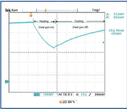
Figure 8. The transient voltage value of the diode includes an exponential curve representing the heating of the external hot air gun (falling curve) and the cooling after removing the hot air gun (rising curve).
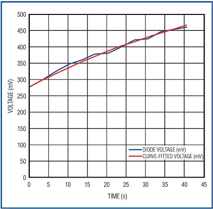
Figure 9. Equation 34, fitted to a pair of diode voltage measurements, very close to the diode measurements after the chip is heated by a hot air gun and then cooled.
As we can see in Figure 9, Equation 34 is very close to the measurement data when kA = -0.0175. In order to verify the correctness of our formula, we tried to fit the decline curve of Formula 28 with the value determined for kA, and the equation was precisely fitted (Figure 10). Therefore, we see that Equation 34 of the system discussed for System Definition 1 is very close to the experimental data.
System definition 2
It is more difficult to verify Equation 30, Equation 31, and Equation 32 of the system 2. It is necessary to generate heat in the die, use the diode forward voltage to measure the die temperature, and fit the temperature value with the C1 voltage simulation data of the proposed RC network. This work can be achieved using MATLAB programming. Given the initial temperature of the entire chip, it is important to record the transient thermal characteristics at different times. In this way, we can also solve the initial capacitance voltage of the RC network. Using the same test setup (see Figure 7), turn on the current channel and collect the diode voltage on the oscilloscope (Figure 11).
Record the transient voltage at three different dissipated powers and simulate these data with a curve. The curve shown in Figure 12 is the fitting result of the first set of data, and the power consumption is 1.626W at this time; the waveform shown in Figure 13 is the comparison between the measured data and the simulated data. Similarly, the waveform shown in Figure 14 illustrates the simulation of the second set of readings (dissipated power 2.02W) by the RC network; the waveform shown in Figure 15 illustrates the simulation of the third set of readings (1.223W). .
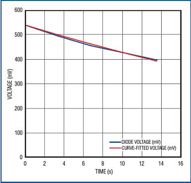
Figure 10. The fitted curve of Equation 28 is very close to the measured diode voltage in the falling part (heating) of the curve. 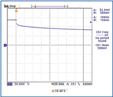
Figure 11. The forward voltage transient of the internal diode of the MAX16828, indicating that the on-chip MOSFET has turned on and generates heat.
The experimental results show that the measured results are in good agreement with the theoretical model. Once the RC network model is built for a specific chip, this model will be very useful for simulating IC transient temperature. The model can also be used for chips of similar size to determine the thermal characteristics at the defined stage. In this way, the working range of the chip can be expressed. In turn, this information can help define the working mode of the chip to avoid overheating.
in conclusion
This article describes the method of simulating the thermal characteristics of the chip through the RC network, and then you can use the SPICE tool to easily simulate. The following methods help to improve the accuracy of the model:
Get data at extreme power consumption conditions and moderate levels. Fitting the RC network to three different conditions at the same time makes the model compound the requirements of most actual power consumption.
Improve the accuracy of the model by collecting data at different ambient temperatures.
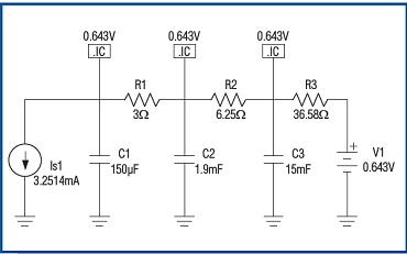
Figure 12. Using the illustrated component values, the RC network can simulate the chip's transient thermal characteristics when heat is generated by the die. 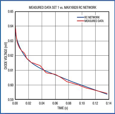
Figure 13. When the die dissipated power is 1.626W, the measured result of the chip heating curve is compared with the fitted curve. 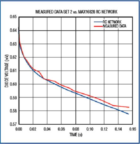
Figure 14. When the die dissipation power is 2.02W, the measured result of the chip heating curve is compared with the fitting curve. 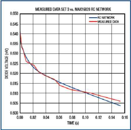
Figure 15. When the die dissipation power is 1.223W, the measured result of the chip heating curve is compared with the fitting curve.
If necessary, accuracy can be improved through experiments, but most applications do not need to know the exact temperature. Application and design engineers and system designers will benefit greatly from this test method. In order to get more detailed chip information, manufacturers can build RC networks for their ICs and use the chip's corresponding SPICE model for verification.
Xinxiang Mina Import & Export Co., Ltd. , https://www.mina-motor.cn