At present, the embedded technology of integrated circuits is developing faster and faster, and various embedded products are becoming more and more popular, especially with large-screen multi-function mobile phones and tablet computers as the typical representative. Low-power microcontrollers (MCUs) play a decisive role. Therefore, the design of CPU as the core MCU has become a mainstream development direction for many universities and major companies to compete in the market. Samsung, FreeScale, Atmel, NXP, TI, ST and other large companies have launched various types of MCUs on a large scale, and each has its own characteristics. Therefore, MCUs with independent intellectual property rights should be different from these big companies in terms of system architecture. Avoid infringement, and second, it is more conducive to market competition. At the same time, product planning should be done: from simple to complex, from single product to series of products, the design platform is continuously maintained and updated, and the level of designers is continuously improved.
Clock and reset scheme design
Clocks and resets play a crucial role in the overall circuit. If there is a problem with these two signals, the circuit will not work properly. Therefore, it is necessary to make a detailed clock scheme and reset scheme, and different clocks need to be provided for different peripherals: a separate clock of USB, a high-speed peripheral such as a CPU, a clock of a low-speed peripheral such as a UART, as shown in FIG.
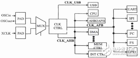
Figure 1 Schematic diagram of the clock scheme
Online debugging solution design
At present, the more commonly used online debugging mode is serial debugging, such as JTAG, EJTAG, UART, etc., using the parallel port, serial port, network port or USB interface of the PC, which makes the online debugging simple and convenient, and the cost is low, as shown in Figure 2. . Since the program to be debugged runs on the target board and the MCU must work normally, it is necessary to design a dedicated debug module to ensure that the host computer software can call the CPU for online debugging of software and hardware, and conform to the IEEE1149.1 protocol standard. The basic structure of this module is shown in Figure 3.
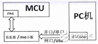
Figure 2 Schematic diagram of a typical online debugging system
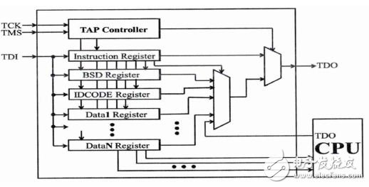
Figure 3 Schematic diagram of the debugging structure
Remote power monitoring system design
The c8051f020 is a mixed-signal soc 8-bit microcontroller that is a fully integrated mixed-signal system-on-chip with an 8051-compatible microcontroller core that is fully compatible with the mcs-51 instruction set. The core adopts a pipeline structure, the machine cycle is reduced from the standard 12 system clock cycles to one system clock cycle, and the execution time of 70% of the instructions is one or two system clock cycles, and the processing capability is greatly improved, and the peak performance can reach 25 mips. At the same time, in addition to the standard 8051 digital peripheral components, c8051-f020 also integrates almost all analog, digital peripherals and other functional components needed to form a single-chip data acquisition and control system. These peripherals or features include: analog multiplexers for multiple analog signals, adc with true 12-bit conversion accuracy, and smbus (i2c compatible), uart, spi, multiple for special functions Multi-function counter/timer, and digital peripherals such as watchdog timer (wdt) and power monitor.
The c8051f020 has a 100-pin tqfp package with low power consumption and a supply voltage of 2.7 to 3.3V. All i/o, rst, and jtag pins are resistant to 5V. Its mcu has 64 general-purpose i/o ports from p0 to p7, and each port pin can be configured as a push-pull output or a drain-open output. For rtl8019as, since its working voltage is 5v, and the operating voltage of c8051f020 is 3.3v, the output of c8051f020 can better drive the oled of 5v input, and additional configuration is needed for the system. In addition to setting the output mode of the corresponding port to “open drainâ€, each port should be connected to the 5v power supply through a pull-up resistor on the circuit. This ensures that the logic “1†output of the c8051f020 can be boosted to 5v. . The MCU uses the c8051f020 chip to continuously read the rtl8019as status register in the query mode. Send or read rtl8019as data in remote DMA mode. See Figure 3 for details.
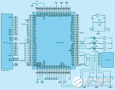
Since the network controller has the ethernet (ieee802.3) protocol processing function, the system can directly connect to the Ethernet via rj45 (and then access the internet through Ethernet). The rj45 connector selected in the system designed in this paper is lf1s022, which already has level shifting function, which simplifies the pcb design. It is worth noting that when designing a pcb, the rj45 connector cannot be too far away from the cpu and the network chip to avoid affecting the data transmission. The rtl8019as tpin+ (59-pin), tpin- (58-pin) pin is a pair of input pins for tp that can receive differential Manchester-encoded data from a twisted pair at a rate of 10 mbits/s. Tpout+ (45-pin) and tpout-(46-pin) are a pair of Manchester-coded differential tp output signals. In order to prevent the twisted pair overload, the output signal will be interrupted in advance, which can reduce congestion. When connected, these four pins are connected to pins 7, 6, 5, and 4 of lf1s022. The other pins of the connector are connected to ground through a capacitor. Finally, a 20mhz crystal oscillator must be connected between pins 50 and 51.
Edit Comment: The composition of embedded device and Ethernet interface, briefly introduces rtl8019as and c8019f chips, and gives the hardware design of embedded mcu and Ethernet control chip. The design takes data acquisition as an example, in industrial production. It has great practical significance, including the design process including clock and reset scheme, online debugging scheme and remote power monitoring system for readers' reference.
The electronic enthusiasts June "embedded technology special issue" invites senior experts from all walks of life to find out with you!
Small computer system interface (SCSI) is an independent processor standard for system level interfaces between computers and intelligent devices (hard disks, floppy drives, optical drives, printers, scanners, etc.). SCSI is an intelligent universal interface standard.
HPCNS SCSI Section
ShenZhen Antenk Electronics Co,Ltd , https://www.antenksocket.com