Introduction to the 555 Timer: The 555 Timer is a versatile integrated circuit that combines both analog and digital functionalities. It is commonly referred to as the 555, and it is typically manufactured using bipolar technology. In CMOS versions, it is known as the 7555. Alongside the single 555 timer, there are dual versions such as the 556 and 7556. One of the key advantages of the 555 timer is its wide operating voltage range, which allows it to function between 4.5V and 16V. The 7555 can operate from 3V to 18V, with an output drive current of approximately 200mA, making it compatible with TTL, CMOS, or analog circuits.
The 555 timer is known for its low cost and reliable performance. It only requires a few external resistors and capacitors to create various pulse generation and conversion circuits, including monostable triggers, astable multivibrators, and Schmitt triggers. Its applications span across instrumentation, household appliances, electronic measurement systems, and automatic control. The internal block diagram and pin configuration of the 555 timer are illustrated in Figures 2.9.1 and 2.9.2, respectively. The internal structure consists of two voltage comparators, three equal resistors in series, an RS flip-flop, a discharge transistor (T), and a power output stage. It also provides two reference voltages at VCC/3 and 2VCC/3.
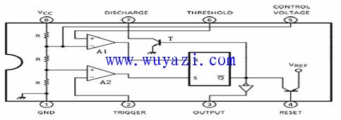
Figure 8-1 Internal block diagram of the 555 timer
How does the 555 circuit work?
The internal block diagram of the 555 timer is shown in Figure 8-1. It includes two voltage comparators, an RS flip-flop, and a discharge switch (T). The reference voltage for the comparators is divided by three 5kΩ resistors, creating reference levels of VCC/3 and 2VCC/3. The output of the comparators controls the state of the flip-flop and the discharge switch. When the input signal exceeds the lower threshold, the output of pin 3 goes low, and the discharge switch turns on. Conversely, when the input signal drops below the upper threshold, the output of pin 3 goes high, and the discharge switch turns off.
The reset terminal (pin 4) is used to force the output to a low level. Normally, this pin is left open or connected to VCC. The control voltage terminal (pin 5) is used to adjust the reference voltage of the upper comparator. A small capacitor (typically 0.01μF) is often connected to ground to filter out noise and stabilize the reference level. The discharge transistor (T) allows the capacitor connected to pin 7 to discharge through a low-resistance path.
Applications of the 555 Timer:
(1) Monostable Multivibrator: A one-shot circuit using the 555 timer and external components R and C is shown in Figure 8-2. A clamp diode (D) is included to protect the circuit. When a negative trigger pulse is applied to the input (pin 2), the output (pin 3) goes high, and the capacitor begins to charge. Once the capacitor voltage reaches 2/3 VCC, the output returns to low, and the capacitor discharges quickly through the discharge transistor. The duration of the output pulse (Tw) is given by Tw = 1.1RC. This circuit is often used for timing functions and can be used to drive relays directly.
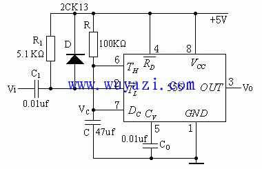
Figure 8-2 555 timer as a one-shot
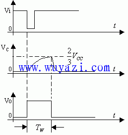
Figure 8-3 Monostable trigger waveform
(2) Schmitt Trigger: By connecting pins 2 and 6 together, the 555 timer can be configured as a Schmitt trigger. As shown in Figure 8-7, the circuit converts a sine wave into a square wave. When the input voltage rises above 2/3 VCC, the output switches to low. When it falls below 1/3 VCC, the output returns to high. The hysteresis of the Schmitt trigger is given by ΔV = 1/3 VCC.
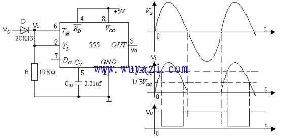
Figure 8-7 555 timer as a Schmitt trigger
(3) Astable Multivibrator: The 555 timer can also be used as an astable multivibrator, generating continuous square waves. As shown in Figure 8-4, the circuit uses resistors R1, R2, and capacitor C to determine the frequency and duty cycle. The capacitor charges through R1 and R2, then discharges through R2. The total period T is calculated as T = 0.7(R1 + R2)C, with the high time being TH = 0.7R2C and the low time being TL = 0.7R2C. The stability of the circuit depends on the precision of the external components.
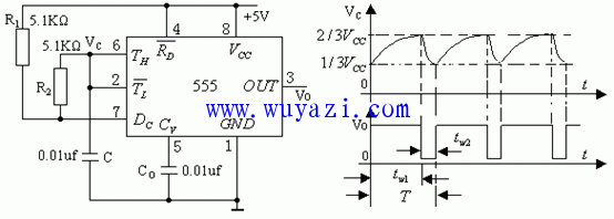 Figure 8-4 555 timer as an astable multivibrator
(4) Adjustable Duty Cycle Multivibrator: To achieve a variable duty cycle, a potentiometer and two diodes are added to the basic multivibrator circuit (as shown in Figure 8-6). Diodes D1 and D2 control the charging and discharging paths of the capacitor. By adjusting the potentiometer, the duty cycle can be set to 50% or other values. This makes the 555 timer suitable for applications requiring precise control over waveform symmetry.
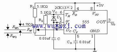
Figure 8-6 555 timer with adjustable duty cycle
Duty cycle = (R2 / (R1 + R2)) × 100%
This flexibility makes the 555 timer a popular choice in many electronics projects, from simple blinking LEDs to complex timing circuits and signal generators.
Mobile Phone Dust Screen,Mobile Phone Matching Products,Computer Mobile Phone Matching Products
SHAOXING HUALI ELECTRONICS CO., LTD. , https://www.cnsxhuali.com