Introduction to the 555 Timer:
The 555 Timer is a versatile and widely used integrated circuit that combines both analog and digital functionalities. It is commonly referred to as the 555, and it is typically manufactured using a bipolar process. In CMOS technology, it is known as the 7555. Alongside the single 555 timer, there are dual versions like the 556 and 7556. One of the key advantages of the 555 is its wide operating voltage range, which allows it to function between 4.5V and 16V. The 7555 can operate from 3V to 18V, with an output drive current of approximately 200mA, making it compatible with TTL, CMOS, or analog circuits.
The 555 timer is cost-effective, reliable, and easy to use. It only requires a few external resistors and capacitors to create various circuits such as multivibrators, monostable triggers, and Schmitt triggers. It is extensively used in applications like instrumentation, household appliances, electronic measurement systems, and automatic control. The internal block diagram and pinout of the 555 timer are shown in Figures 2.9.1 and 2.9.2 respectively. The internal structure includes two voltage comparators, three resistors in series, an RS flip-flop, a discharge transistor (T), and an output stage. It provides two reference voltages: VCC/3 and 2VCC/3.
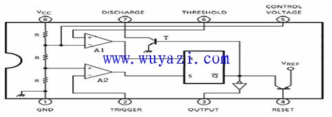
Figure 8-1 Internal block diagram of the 555 timer
How does the 555 circuit work?
The internal block diagram of the 555 timer is shown in Figure 8-1. It consists of two voltage comparators, an RS flip-flop, and a discharge switch (T). The reference voltage for the comparators is divided by three 5kΩ resistors, creating two reference levels: VCC/3 and 2VCC/3. The outputs of the comparators control the state of the flip-flop and the discharge switch. When the input signal exceeds the lower threshold (VCC/3), the output at pin 3 goes low, and the discharge switch turns on. Conversely, when the input signal drops below the upper threshold (2VCC/3), the output goes high, and the discharge switch turns off.
The reset terminal (pin 4) is active-low. When it's pulled low, the output of the 555 goes low. Normally, this pin is left open or connected to VCC.
Vc (pin 5) is the control voltage terminal. It is usually set to VCC/3 as the reference for comparator A1. If an external voltage is applied to this pin, it changes the reference level, allowing for additional control over the output. A 0.01µF capacitor is often connected between pin 5 and ground to filter out noise and stabilize the reference voltage.
T is the discharge transistor. When it is turned on, it provides a low-resistance path for the capacitor connected to pin 7 to discharge.
555 Timer Applications:
(1) Monostable Multivibrator (One-Shot)
The circuit is shown in Figure 8-2, where the 555 is used with external timing components R and C. A clamp diode D is also included. When the circuit is in a stable state, the internal discharge transistor T is on, and the output Vo is low. When a negative trigger pulse is applied to the input (pin 2), the voltage at pin 2 drops below VCC/3, causing the comparator to activate. This starts the charging of capacitor C, and the output switches to high. Once the capacitor charges above 2VCC/3, the comparator resets the flip-flop, and the output returns to low. The capacitor discharges through the transistor, ending the transient state. The waveform is shown in Figure 8-3.
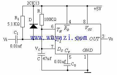
Figure 8-2 555 constitutes a one-shot
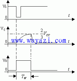
Figure 8-3 Single-state trigger waveform
The duration of the temporary state (T_w) depends on the values of R and C:
T_w = 1.1RC
This delay can be adjusted from microseconds to tens of minutes by varying R and C. The monostable configuration can drive a relay directly, and the reset terminal can be grounded to terminate the pulse. A flyback diode is often used across the relay coil to protect the internal transistor from back-EMF.
(2) Schmitt Trigger
The circuit is shown in Figure 8-7. By connecting pins 2 and 6 together, a Schmitt trigger is formed. As the input voltage (Vi) increases, the output (Vo) changes when Vi crosses the upper threshold (2VCC/3). When Vi decreases below the lower threshold (VCC/3), the output switches again. This creates a hysteresis effect, making the circuit ideal for signal conditioning and noise filtering.
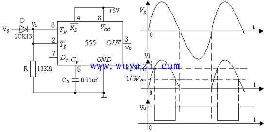
Figure 8-7 555 constitutes a Schmitt trigger | Figure 8-8 555 constitutes a Schmitt trigger waveform
(3) Astable Multivibrator
As shown in Figure 8-4, the 555 forms an astable multivibrator using external resistors R1, R2, and a capacitor C. Pins 2 and 6 are connected together. There are no stable states; the circuit continuously oscillates. The capacitor charges through R1 and R2 and discharges through R2, causing the output to toggle between high and low. The resulting waveform is a square wave, as shown in Figure 8-5.
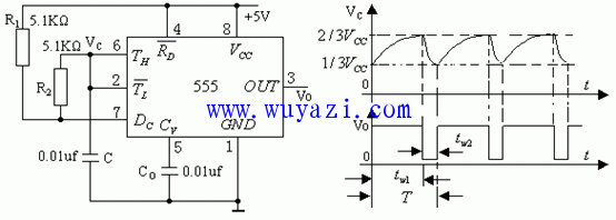 Figure 8-4 555 constitutes a multivibrator | Figure 8-5 Waveform of a multivibrator
The time parameters are given by:
T = 0.7(R1 + R2)C
T1 = 0.7R2C
R1 and R2 should each be at least 1kΩ, but their sum should not exceed 3.3MΩ. The stability of the external components determines the stability of the oscillation. The 555 timer is known for its simplicity, precision, and strong output capability, making it a popular choice for many applications.
(4) Adjustable Duty Cycle Multivibrator
By adding a potentiometer and two diodes to the circuit in Figure 8-4, the duty cycle of the output can be adjusted. Diodes D1 and D2 control the charging and discharging paths of the capacitor. When D1 is on, the capacitor charges through R1 and R2, while D2 controls the discharge path through R2. This allows for independent control of the high and low periods of the waveform.
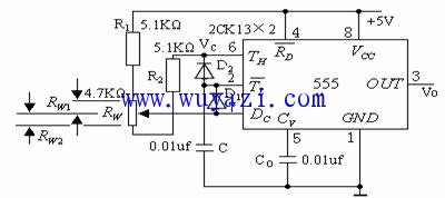
Figure 8-6 555 constitutes a multi-vibrator with adjustable duty cycle
The duty cycle can be calculated as:
Duty Cycle = (R2 / (R1 + R2)) × 100%
If R1 equals R2, the output is a 50% duty cycle square wave, which is useful in many digital applications.
Mobile Phone Dust Screen,Mobile Phone Matching Products,Computer Mobile Phone Matching Products
SHAOXING HUALI ELECTRONICS CO., LTD. , https://www.cnsxhuali.com