Foreword
In modern wireless communication systems, there is an increasing demand for high-capacity, high-speed data wireless transmission. Many manufacturers have also introduced RF ICs based on 802.11 series protocols, and widely used technologies such as wireless routers and Bluetooth, for 2.4GHz. The use of frequency bands is increasing, but except for some high-end signal generators with signal generation in the 2.4 GHz band, most common signal generators do not involve the 2.4 GHz band. The development involves an RF signal generator based on the 2.4 GHz band to meet The need for scientific research and teaching instruments. This article is based on this, low-cost, reliable performance of the 2.4GHz band RF signal generator.
System solutions
The system scheme uses the human-machine control on the instrument panel to set the operating frequency and baseband modulation mode to be directly controlled by the FPGA to generate four basic modulation modes, namely QPSK, 16/64-QAM, GMSK, FSK, and baseband. The I/Q two signals are serially converted and sent to the AD9856 to modulate the signal to a 70MHz IF signal, then mixed to the 2450MHz RF signal by the upmixer MAX2671, and then the mixed signal is sent to the RF filter. The signal is then output by a controllable gain amplifier.
The block diagram of the RF signal generator in the 2.4 GHz band is shown in Figure 1.
Circuit design
The signal modulation circuit is firstly designed by FPGA circuit using ALTERA's EP1C20 chip. VHDL programming is used to output control information from the human-machine interface, and then the control information is corresponding to the signal to be generated, and the signal is output to the AD9856. The AD9856 is a single-chip mixed-signal 12-bit integrated digital upconverter from Analog Devices, Inc., with a sampling rate of 200 MSPS, producing an 80-MHz digital output and a 80 dB narrowband spurious-free signal dynamic range. The AD9856 features an internal 200MHz clock and an integrated 4-20x programmable clock multiplier with a lock indicator that provides a high-precision system clock, single-ended or differential input reference clock, and can output a data clock; internal 32-bit quadrature DDS, FSK modulation function can be realized; 12-bit DDS and DAC and data path structure can accept composite I/Q input data; 32-bit frequency control word adopts SPI-compatible interface, and FPGA control is reliable and convenient, serial clock is 10MHz; with inverted SINC function, recovers the desired signal envelope before DAC conversion. The block diagram of the modulation signal generated by the AD9856 is shown in Figure 2.

Figure 1 system block diagram

Figure 2 AD9856 circuit that produces a modulated signal
As can be seen from Figure 2, the code modulation is performed in the FPGA, and the generated I/Q signals are sent to the AD9856 through serial-to-parallel conversion. There is a DDS core inside the AD9856, and the orthogonal local oscillator signal is generated through the FPGA control. Into the quadrature modulator, each channel is multiplied by the I/Q signal and then added to generate a quadrature modulation signal, and the specific modulation mode can be designed through the baseband signal coding mapping of the FPGA, and finally through the 12-bit DAC. The quadrature-modulated analog differential signal output is then converted into a single-ended signal by a coupled RF transformer, filtered by a 70MHz SAW filter, and finally amplified by an intermediate frequency amplifier for feeding to the mixer. Mixed up.
Mixer circuit
The mixing circuit is extremely important for the implementation of the 2.4GHz frequency band. It mainly completes the modulation of the 70M IF signal to the 2.4GHz RF, and requires the band suppression type of the mixing circuit. Here, the MAX2671 mixing chip of the dedicated 2.4GHz band of MAXIM is used. The MAX2671 allows an IF input frequency between 40MHz and 500MHz and an RF output frequency between 2.4GHz and 2.5GHz. Single-ended signal is integrated with a single-channel multiplier. It has a gain of 8.9dB when the 2450MHz RF signal is mixed. Therefore, the local oscillator signal can be between -10dBm and +5dBm. When the input and output are matched, only a few peripheral devices are needed, and the circuit structure is shown in FIG.
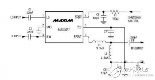
Figure 3 MAX2671 circuit
RF local oscillator signal circuit design
In the signal generator design, to mix the 70MHz IF signal to the RF signal of the 2450MHz ISM band, it is necessary to generate the RF local oscillator signal at a frequency of 2380MHz. The local oscillator signal circuit uses the phase-locked loop of PLL+VCO to provide the local oscillator signal, which has the advantages of high precision, high stability, variable frequency, etc., and is convenient for adjusting or expanding the frequency resources in the future. The frequency stability of the local oscillator signal is very important. This part is designed with the integrated circuit as the core. It uses the frequency synthesizer ADF4113 from ADI and the MAX2750 voltage-controlled oscillator from MAXIM. The block diagram is shown in Figure 4.
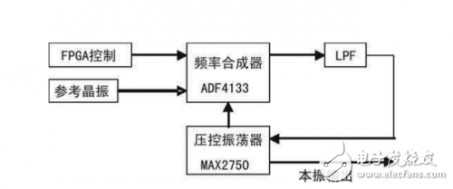
Figure 4 RF local oscillator signal circuit block diagram
In order to control the frequency synthesizer to control the phase-locked loop frequency synthesizer ADF4113 through FPGA analog 3-wire serial interface signal timing, the frequency of the reference crystal oscillator and the frequency of the voltage-controlled oscillator (VCO) are completed according to the ADF4113 internal (the N-divider is divided) The phase difference is compared and converted into a corresponding linear voltage output. After high-frequency interference is considered by the low-pass filter (LPF), a relatively stable voltage is obtained, and the oscillation frequency output of the VCO is controlled, thereby obtaining the required 2380MHz local oscillator signal.
The ADF4113 is a high performance frequency synthesizer from Analog Devices, with a maximum operating frequency of 4 GHz. The ADF4113 consists primarily of a low noise digital phase detector (PFD), a precision charge pump, a programmable reference divider, programmable A (6bit) and B (13bit) divide counters and a dual mode divider (P /P+1) constitutes. The MAX2750 is a voltage-controlled oscillator used by MAXIM for the 2.4GHz to 2.5GHz ISM band. It operates in the 2.4GHz to 2.5GHz ISM band. The circuit structure is shown in Figure 5.
The role of the LPF is to take into account the high frequency interference of the voltage, thus obtaining a relatively stable voltage. The design of the LPF can be implemented by a dedicated program-controlled filter chip. For example, the MAX297 can be used to adjust the low-pass cut-off frequency. The cutoff frequency is 0-50KHz, which makes the design more flexible. The other way is to use the standard 3rd order no. The source loop filter is designed with an LRC circuit.
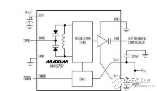
Figure 5 MAX2750 circuit diagram
Design test
Determine the test frequency and input and output dB values ​​at all levels to complete system debugging. The IF signal power entering the MAX2671 is -30dBm to -20dBm, and the RF local oscillator signal power is -10dBm to +5dBm. Through testing, the output spectrum of the RF local oscillator signal circuit is shown in Figure 6. As can be seen from the figure, the output power of the signal source reaches -9dBm, which can fully meet the requirements of the MAX2671 RF local oscillator signal input between -10dBm and +5dBm. As can be seen from the figure, the output power of the signal source reaches -24.5dBm, which can fully meet the requirements of the IF signal input of the MAX2671 of the upper mixer between -30dBm and -25dBm.
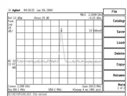
Figure 6 2380MHz RF LC signal spectrum
Figure 7 shows the signal spectrum output from the mixer MAX2671. The 70MHz IF signal is mixed with the 2380MHz RF LO signal to output the 2310MHz and 2450MHz upper and lower sideband signals. The lower frequency component of 2310MHz is filtered out by the RF dielectric filter. The desired 2450MHz useful signal is obtained, the output power is set by the adjustable power amplifier, and then sent to the N-type head output.
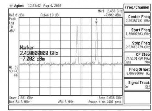
Figure 7 Output signal spectrum of the MAX2671
Conclusion
The 2.4GHz RF signal generator is designed to meet the wide application of wireless communication, wireless LAN, etc., with low cost, simple peripheral circuit, stable working frequency band, adjustable parameters, friendly human-machine interface, and operation. The ordinary signal generator is as convenient as it can meet the application requirements of test instruments, teaching and scientific research.
1U,8 Ways Aluminum Shell, Rackmount 19'' Inch 16A 250V PDU (Power Distribution Unit)
Features:
- 19" Horizontal/Vertical Mount Type
-
Heavy Duty Aluminuml Body Or ABS- 1U,1.5U size
-
Shell Material:Uninflammable PC modules,Aluminum/ABS Alloy Shell
-
Type of Cable & Plug:3G*1.5mm2*2m,DIN49441 Plug
-
Protection:Optional Security System To Avoid Accidental Disconnections.
-
Certificates:CE-EMC;CE-LVD;RoHS;UL94-VO
-
Different Types of Input Male Plug Top Options are available
Technical Specifications:
- Rated Current:16A
-
Max Output Power:4000W
-
Rated Voltage:250V,Household Voltage 240V 50/60Hz
-
Switch:Red On/Off
-
Color:Black Or Aluminum White
-
Other Functions For Option
Application:
Used for power distribution for 19 inch 1 U server rack.
Product Images:

Power Distribution Unit
Intelligent Management System(Appdu),Appdu â… (Without Intelligent Management),Appdu â…¡(With Intelligent Management),Pdu (Power Distribution Unit)
Guangdong Steady Technology Co.LTD , https://www.steadysmps.com