We provide all sets of sparts for ST45(DW45) and finished products;
ST45(DW45)series intelligent air circuit breaker (hereinafter called ACB) are applied to the network circuit of AC 50 Hz, rated voltage 400V, 690V and rated current between 400A and 6300 A. Mainly used foe distributing energy and protecting the circuit and power supply device against short-circuit, under-voltage, single-phase ground fault, etc. The ACBS has intelligent protection function and the key parts adopt intelligent release. The release can make the accurate selective protection, which can avoid cutting off the power and improve the reliability of power supply.
The products conform to IEC60947-2, IEC 60947-4 standards.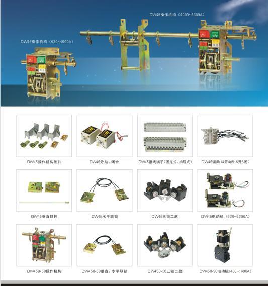
Â
Via In Pad PCB
What is Via In Pad? In shortly,via in pad is the via holes are at the SMD pad.The vias are very small,usually under 0.3mm.Why and how? First is there is no enough space to layout,you have to put the vias and holes closer even together.Second it helps thermal management and for high frequency boards,it may help improve signals.
Because the SMD pads are for SMD components loading,so the solder can not flow to inner layer or the other side when assemble.That is the most important for via in pad board.
How PCB manufacturers like us to do via in pad board? We will fill all vias with non-conductive epoxy and plate copper over it ,so the vias are flat same as others. Many PCB factories are unable to do such capability.
The key technology is how we fill vias and guarantee there is no any solder (surface finishing) in the holes.
Filled via in pad is a way to achieve intermediate density with an intermediate cost compared to using blind/buried vias. Some of the key advantages associated with using the via in pad technology are:
.Fan out fine pitch (less than .75mm) BGAs
.Meets closely packed placement requirements
.Better thermal management
.Overcomes high speed design issues and constraints i.e. low inductance
.No via plugging is required at component locations
.Provides a flat, coplanar surface for component attachment
Via in big pads are not a big problem.but for BGA,that is technology.As BGA pads are very small,10mil or 12mil,and there is no enough space.Manufacturing is not easy as other boards.
Via In Pad PCB
Via In Pad PCB,6Layer Via In Pad PCB,Touch Pad PCB,Via In Pad
Storm Circuit Technology Ltd , http://www.stormpcb.com