1 Introduction
Many embedded systems, especially some embedded systems with more frequent human-computer interaction (HMI), are the most widely used input devices. Due to the heterogeneity of embedded devices, it is not feasible to provide a universal keyboard. Generally, it is necessary to design a special keyboard according to the actual function of the embedded system and implement the corresponding driver.
The common way to extend the keyboard on an embedded device is through the use of the CPU's GPIO port scan. Obviously, this method will take up the system's GPIO resources, especially in systems where the GPIO resources are tight and the buttons are more. It is especially prominent. Of course, it can also be realized by externally expanding GPIO (such as 8255, etc.) or by externally extending a dedicated keyboard interface (such as 8279, etc.), but this method obviously increases the complexity of the system, and is quite inconvenient in actual system design.
This paper takes a POS machine keyboard (8&TImes;8) on ARM9 (AT91RM9200) embedded microprocessor as an example, and presents a new design idea of ​​extending multi-row keyboard on embedded device, and realizes it in ARM-Linux system. The keyboard driver.
2, the hardware design of the interface circuit
This article uses a design example to illustrate how to use a simpler way to implement an 8&TImes;8 POS machine matrix keyboard. The microprocessor used in the POS machine is the AT91RM9200 chip. AT91RM9200 is a high performance 32-bit ARM9 processor produced by ATMEL. It is a general-purpose industrial grade ARM chip, which has been widely used in industrial control, intelligent instrumentation and other fields [3, 4]. The chip characteristics can be found in the literature [2].
Extending the keyboard on the AT91RM9200 is usually done through its GPIO port. Although the AT91RM9200 provides 4 & TImes; 32 programmable GPIO ports. However, in order to reduce chip size and power consumption, many of its GPIO ports are multiplexed with the system's peripheral device controller ports or address lines and data lines, so there are very few GPIO ports that can be used for expansion. For an 8&TImes;8 keyboard, if the traditional GPIO port expansion method is used, 16 GPIOs are needed, which is difficult to satisfy in a more complicated POS system, so other methods are needed to solve this problem.
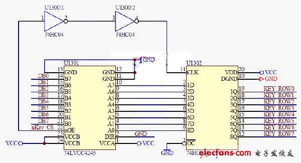
Figure 1 keyboard interface schematic
In this paper, the data latching method makes full use of the data width advantage of the 32-bit processor, and uses the data line to replace the GPIO port required for keyboard expansion, thereby reducing the occupation of system GPIO resources. The implementation principle of the keyboard interface is shown in Figure 1. In the circuit shown in Figure 1, U1301 (74LVCC4245) is a three-state buffer, U1302 (74HC574) is a latch, the system works as follows:
The nOE terminal of U1301 is connected to the decoding output nKey_CS of the system. The component address is determined by the system decoding circuit. When writing data to the address, the nKey_CS signal is low level, the data can pass U1301, and the nKey_CS signal is inverted by two stages. After the delay, the data is latched as a latch signal to the output of U1302 as the line scan signal of the keyboard, while the column scan signal of the keyboard still uses the system's GPIO. The keyboard is scanned by sending a low level signal to each line in turn and detecting the column signal connected to the GPIO. In this system, only the lower 8 bits of the 32-bit data of the system are used as the line scan signal. In the case of implementing the 8×8 matrix keyboard scan, only 8 GPIO ports are needed. If the same method is used, 16 are used respectively. Bit data or 32-bit data as a line scan signal requires only 4 or 2 GPIOs. Obviously, this method can greatly save the system's GPIO resources compared with the conventional method.
3, the keyboard driver module design
After completing the design of the interface circuit, you need to write the corresponding keyboard driver module. This article uses the ARM-Linux operating system in the AT91RM9200 chip, which provides great convenience for the development of the keyboard driver. The keyboard driver module can be divided into three parts: hardware initialization, file operation function implementation and keyboard scanning program.
3.1 Hardware Initialization
The development mode of the keyboard driver is similar to the driver development process of the general character device in the Linux system. For a detailed analysis of the Linux device driver development, refer to the literature [1]. The first thing to do is the initialization function and the clear function of the driver module. In the initialization function, in addition to completing the module registration, hardware initialization should also be performed. The following is the pseudo code of the hardware initialization in the initialization function of the module according to the characteristics of the GPIO controller of the AT91RM9200 chip [2].
......
Set the GPIO port used for GPIO controller control
Set the type of GPIO port used as input
Enable input glitch filtering for the GPIO port used
Enable the corresponding GPIO controller clock
Take the virtual address of the specified address and write data to the address 0x0
48V Ebike Battery,48V Ebike Battery Series,48V Rechargeable Battery,Ebike Litthium Battery
ZHEJIANG TIANHONG LITHIUM-ION BATTERY CO.,LTD , https://www.tflbattery.com