Design of Power Line Carrier Communication Module Based on ST7538 and ATmega88V
The low-voltage distribution network is an energy transmission network with the most users and the widest distribution. Power line carrier communication is a communication method that uses the existing power line network for information transmission. It can be used for power management, lighting control, heating and cooling system control, remote meter reading, alarm system and intelligent community. The advantage of using power line as a communication medium is that it does not require rewiring, is easy to maintain, and greatly saves communication costs. This paper designs a set of power line carrier communication module based on the modulation and demodulation module ST7538 and ATmega88V microcontroller.
The overall design of the system is based on the system principle of low-voltage power line carrier communication, giving the overall design of the entire system, as shown in Figure 1. The power line carrier communication node module mainly includes the following parts: a microcontroller part, a signal processing part, a power supply circuit part and a power line interface part.
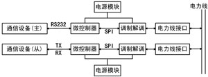
Figure 1 System principle of low-voltage power line carrier communication
hardware design
1 The choice of microcontroller The microcontroller is the control core of the system, which is responsible for the coordination and scheduling of tasks in the entire system. In order to overcome many unfavorable factors such as large signal attenuation, large time variability, and noise impact on the power line, some coding and decoding schemes with strong error correction capabilities need to be adopted, but this may increase the complexity of the algorithm and reduce the operation speed. After comprehensive consideration of cost and computing power, the microprocessor chose the high-performance, low-power 8-bit AVR series microcontroller ATmega88V. For its specific parameters and characteristics, please refer to the product manual.
2 Modulation and demodulation chip selection Signal modulation and demodulation as well as adaptive balanced amplification of the signal, filtering and communication with the microcontroller and other functions are completed by the power line carrier chip. The power line interface functions as coupling, isolation, filtering and protection.
Therefore, we choose the ST7538 carrier chip as the signal modulation and demodulation chip. ST7538 carrier chip is a half-duplex, synchronous / asynchronous, FSK modem chip designed for power line network communication in the home and industrial fields. It has the characteristics of powerful functions, high integration, and many anti-interference technologies. It is already in power carrier communication More widely used.
ST7538 exchanges data with the main controller through the serial interface. Because the USART of ATmega88V is used to communicate with the server in the scheme design, the interface between ST7538 and the host uses its serial interface to communicate with the serial peripheral interface SPI of ATmega88V to achieve. ATmega88V's serial peripheral interface SPI has the characteristics of full-duplex, 3-wire synchronous data transmission, master-slave and operation. In this scheme design, ST7538 is used as the master, ATmega88V is used as the slave, and the data synchronization transmission clock is provided by ST7538.
3 The choice of power chip Because the working voltage of the main chip (ST7538, ATmega88V) in the whole system is 12V and 5V, the total power of the system does not exceed 2W, so we choose LM2596 as the power chip. The LM2596 switching voltage regulator is a step-down power management monolithic integrated circuit. It has a very small voltage regulation rate and current regulation rate. It has a 3A load drive capability. The LM2596 can output 3.3V, 5V, 12V, 15V fixed voltage and Adjustable voltage output mode with adjustable voltage, the input voltage reaches 36V. LM2596 is relatively simple in application and has few peripheral components, as shown in Figure 2 (only four), built-in frequency compensation circuit and fixed frequency oscillator. The switching frequency of the LM2596 series products is 52kHz, so a small filter element can be used in the application. It can effectively replace the general three-terminal linear regulator, and can fully reduce the area of ​​the heat sink. Under the specified input voltage and output load, the error range of the LM2596 output voltage is ± 4%; the oscillation frequency error range of the oscillator is ± 10%; the typical standby current is 50μA, the chip has built-in overcurrent protection circuit and overheating protect the circuit. Therefore, two pieces of LM2596 were selected in the design as two branches to output 5V and 12V respectively. In addition, in the PCB design, it is considered that the switching power supply chip will generate strong electromagnetic wave radiation, so try to stay away from the modulation and demodulation circuit and the filter circuit, so as not to cause interference to the carrier signal.
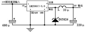
Figure 2 LM2596 power module circuit principle
4 Power line interface circuit design The key to realizing high-quality and efficient power line carrier communication lies in the selected carrier modulation and demodulation module and the corresponding interface circuit. The power line interface circuit couples the modem part to the power line to realize the transmission of the signal on the power line. The communication process requires this interface circuit to filter the signal when sending the signal, to filter out certain noises such as second harmonics, and to make the signal have enough power to be coupled to the power line through the power amplifier; The noise in the signal is filtered, and the signal is amplified, and then the signal is transmitted to the modulation and demodulation module for demodulation. Therefore, the performance of the interface circuit determines the quality of the communication effect. Generally, the power line interface circuit includes: receiving part, transmitting part, power amplifying part and protection part. Because ST7538 has a power amplifier circuit inside, it only needs to design three parts of receiving, transmitting and protecting. The power line interface circuit is shown in Figure 3.
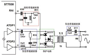
Figure 3 Power line interface circuit
In the transmitting circuit, the values ​​of capacitor C11, inductor LC12, inductor L4 and equivalent inductive impedance LC are generally given in advance, and the values ​​of capacitors C13 and CR9 need to be determined by calculation. When selecting the values ​​of C11, LC12, L4 and LC, pay attention to the leakage inductance of the transformer, the capacitance of the crystal diode and the equivalent series resistance ESR (100mΩ ~ 1Ω) of the series device (C13, LC12, T1, L4, C11) So use resistive devices as much as possible. The transformer uses 1: 1 isolation transformer. The impedance condition of the analog power line is to add an inductive load to the output of the filter, so that its impedance characteristic is 2LC = 100μH. The ESR of the inductive device in the circuit should be proportional to its inductance, and the ESR of the inductive device should be as small as possible. The inductance selects LBC (large spool with winding core), the inductance value is as small as possible, so the value of LC12 is selected as 10μH, and the value of L4 is selected as 22μH. The role of C11 is to isolate the transformer from the power line, filter the 50 / 60Hz signal on the power line, prevent low-frequency signals from entering the circuit and let some high-frequency signals pass, select X2 type capacitors, this capacitor has short circuit protection function, so C11 The value is generally selected as 33nF / 400V. According to the pole frequency formula, the calculated value of C13 is 220nF, and the value of CR9 is 100nF.
The passive filter used in the receiving circuit is better than the active filter, because the active filter will produce a white noise equivalent to the received signal. A parallel resonant circuit is adopted, and a second-order passive band-pass filter (C36, L7, R11) is used. The frequency of the receiving filter is mainly determined by the values ​​of capacitor C36, inductor L7 and resistor R11. The center frequency can be set to 132.5kHz. An important factor for the performance of the filter is the quality factor Q, and the Q value is selected from 2 to 3. Use a polypropylene capacitor with a tolerance of 5% and a BC (spool with winding core) inductance of 10%. In order not to affect the transmission part and reduce the DC current through the primary coil of the transformer, the value of R11 should be as large as possible, but if the value of R11 is too large, a higher white noise will be generated, so the value of R11 is taken as 750Ω. Keep the value of R11 unchanged, and different values ​​of C36 and L7 can be obtained according to the selection of center frequency and quality factor.
In the protection circuit part, a bidirectional voltage regulator tube is generally used. When the voltage value is not less than the voltage of the voltage regulator tube, the voltage regulator tube will be shorted to ground, thereby protecting the device of the interface circuit from being burned out. The interference between the live line and the neutral line is differential mode interference, the common line interference between the live line and the ground line, and the neutral line and the ground line. The use of a bidirectional voltage regulator only affects the differential mode spike signal and has no effect on the common mode spike signal. When the common mode spike signal appears, it will cause damage to the circuit, so here three diodes (D16 and D15 are P6KE6V8, D17 is SM6T6V8A), connecting them into a star-shaped structure. For the differential mode spike signal, D16 and D15 form a bidirectional regulator tube. For the common mode spike signal, this star structure is equivalent to two bidirectional regulator tubes (D15 and D17, D16 and D17).
Software design When the system is started, after the program is initialized, it will automatically enter the state of receiving data from the power line, and start to detect the presence and correctness of the carrier signal. If the carrier signal is detected and correct, the system enters the carrier receiver interrupt program and starts to receive data from the power line; if there is no carrier signal at the beginning, the system starts to detect the serial port to determine whether there is data transmitted from the serial port. As for data, the system enters the serial port data receiving state. After confirming that the serial port data reception is completed, it immediately enters the carrier transmission interruption program to complete data modulation and transmission. If there is no data transmission between the power line and the serial port, the system re-enters the detection state, restarts the detection of the power line, and enters a new cycle. The flow chart is shown in Figure 4. In order to avoid the serial port being in the receiving and sending state at the same time, causing data conflicts, the status word query and interrupt settings are completed in the program.
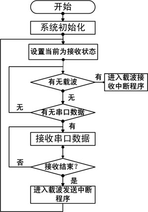
Figure 4 Program flow of power carrier communication system
Conclusion The circuit design scheme based on ATmega88V and ST7538 low-voltage power line carrier communication module introduced in this article has the characteristics of simple structure, low cost, flexible and reliable working mode, and strong anti-interference ability. After experimental observation, the equipment is running well, the data transmission is stable and reliable, and it can automatically restart in the event of a failure.
Rj45 Coupler,Rj45 Surface Mount Jack,Electrical Cable Couplers,Phone Connector Wiring
Dongguan Fangbei Electronic Co.,Ltd , https://www.connectorfb.com