Design of wireless communication module based on CC1020
This article introduces a communication module based on the wireless transceiver chip CC1020 with C8051F310 microcontroller as the control core. The working principle and working method are analyzed, and the design idea and hardware circuit are given. And focuses on the implementation process of the communication module.
Keywords: wireless communication; CC1020; radio frequency; C8051F310
introduction
With the rapid development of network and communication technology, wireless communication has broad application prospects in many fields due to its low cost, good scalability, less geographical constraints, simple and flexible installation and construction.
CC1020 Introduction
CC1020 is an ideal UHF monolithic transceiver chip. It is mainly used in the ISM (Industrial, Scientific and Medical) frequency band and SRD (Short Range Device) in the 426/429/433/868 / 915MHz frequency band. It can also be used for the frequency of 402MHz ~ 470MHz after programming. Multi-channel equipment from 804MHz to 940MHz. The main working parameters of CC1020 can be programmed through the serial bus interface, such as output power, frequency and AFC.
In the receiving mode, CC1020 can be regarded as a traditional superheterodyne receiver. The RF input signal is amplified by low-noise amplifiers (LNA and LNA2), and then reversed through an integrator (I and Q) to generate an intermediate frequency IF signal. In the intermediate frequency processing stage, the I / Q signal is mixed, filtered, amplified and converted into a digital signal by the ADC. Then carry out automatic acquisition control, channel filtering, demodulation and binary synchronization processing, output digital demodulation data on the DIO pin, and acquire synchronous digital clock data on the DCLK pin. RSSI is in digital form and can be read out through the channeling interface. RSSI can also be used as a programmable carrier detection indicator.
In the transmission mode, the synthesized RF signal is directly fed to the power amplifier PA. The RF output is a FSK signal, which is generated by FSK modulation from the digital bit stream fed to the DIO pin. A high frequency filter can be used to obtain Gaussian frequency shift keying GFSK. The transceiver circuit inside the chip makes the antenna easy to access and match.
Hardware circuit design
Microcontroller selection
The microcontroller uses the C8051F310 produced by Cygnal, which has a CIP-51 core fully compatible with 8051. Single-ended / differential ADC, hardware-implemented I2C, enhanced UART and SPI interface, Flash memory has in-system reprogramming capability, can be used for non-volatile data storage, and allows 8051 firmware to be updated in the field. This type of single chip microcomputer is small in size and high in performance. It can quickly access data and is easy to system development and expansion. It is very suitable for the needs of this design.
CC1020 structure configuration interface
The connection of CC1020 structure configuration interface and microcontroller is shown in Figure 1. The microcontroller uses pins P2.2 ~ P2.5 to connect with the structure configuration interface PSEL, PCLK, PDI, PDO of CC1020. The PDO is connected to an input of the microcontroller. PDI, PCLK and PSEL are connected to the output of the microcontroller. If PDI and PDO are connected together, the microcontroller can use a bidirectional pin terminal, which can save an I / O port of the microcontroller.
When the structure configuration interface is not used, the microcontroller pins connected to the PSEL, PCLK, PDI, and PDO pins can be used for other purposes. When the PSEL pin terminal is inactive (maintains a high level) (the PSEL pin terminal is active low), PCLK, PDI, and PDO are high-impedance input states. The PSEL has an internal pull-up resistor, which must be turned off in low-power mode (controlled by the microcontroller tristate) or set to a high level to prevent current from flowing into the pull-up resistor.
CC1020 is programmed through a simple four serial SPI interface. There are 8-bit structure configuration registers. The address of each register is 7 bits, and 1 bit is used as a read / write bit to initiate a read or write operation. The complete configuration of CC1020 requires 33 data frames to be sent, each with 16 bits (Address 7 bits, R / W 1 bit, Data 8 bits). The time required for a complete configuration depends on the frequency of PCLK. If the PCLK frequency is 10MHz, the time to complete a complete configuration is less than 53ms. Set CC1020 to low power consumption mode, only need to send one frame of data, so the time required is less than 2ms. All registers are readable.
CC1020 signal transceiver interface
The connection between the CC1020 signal transceiver interface and the microcontroller is shown in Figure 1. The microcontroller uses pins P2.6 and P3.4 to connect to the CC1020's bidirectional synchronous data interfaces DIO and DCLK.
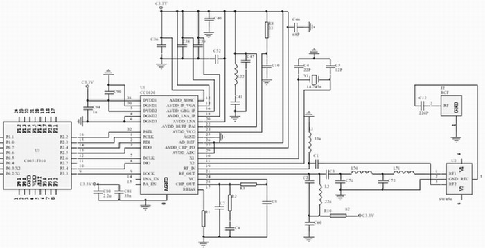
Figure 1 CC1020 and microcontroller connection circuit
A bidirectional pin of the microcontroller is connected to the DIO of CC1020 for data transmission and reception (input and output). DCLK provides data timing and must be connected to an input of the microcontroller.
Data output can choose to use a separate pin. At this time, set SEP_DI_DO = 1 of CC1020's INTERFACE register. In synchronous mode, the LOCK pin is used for data output, and the DCLK pin is used for data output in asynchronous mode, and the DIO pin terminal is only used for data input.
One pin of the microcontroller can be used to monitor the lock signal of the phase-locked loop, that is, the LOCK pin signal. When the phase-locked loop is locked, the LOCK pin is at a logic low level. It can also be used for carrier detection and monitoring of other internal test signals.
CC1020 can be set to three different data transmission forms: synchronous NRZ mode, synchronous Manchester code mode and asynchronous transmission UART mode. These three modes have their own characteristics.The synchronous Manchester code has the best anti-interference ability, but the baud rate is doubled, the asynchronous transmission UART is the simplest to implement, but the anti-interference ability is the worst, and the synchronous NRZ anti-interference ability is better than UART However, it is slightly worse than the synchronized Manchester code, and the difficulty of implementation is somewhere in between. Considering that the microprocessor basically supports UART serial communication, so this mode is selected, and the test results can fully meet the requirements.
CC1020 antenna selection
CC1020 can use a variety of antennas. The antennas commonly used in short-range communication are monopole antennas, helical antennas and loop antennas. This design uses the best and simple 1/4 wavelength monopole antenna.
Power management
CC1020 provides very flexible power management to meet the stringent requirements for power consumption in battery-driven applications. The low power consumption mode is controlled by the MAIN register and the POWERDOWN register. There are independent bits in the MAIN register, which are used to control the receiving part, transmitting part, frequency synthesizer and crystal oscillator. This independent control method makes the power consumption of each application can be optimized to a minimum. Because this design is a separate wireless communication module, the requirements for power consumption are not too strict. The system uses 5V power supply and outputs 3V voltage stably through NCP500.
Anti-interference measures
The wireless RF transceiver system is very sensitive to power supply noise, so the design adopts the method of separate power supply from the wireless RF part and other circuits. High-frequency devices are sensitive to noise, so filters or voltage regulators are added to each part of the power supply to reduce the interference of power supply noise on the chip. In addition, power monitoring and watchdog circuits are used on the chip to greatly improve the anti-interference performance of the entire circuit.
Chipcon provides the circuit reference design of the radio frequency part. The layout of the radio frequency part refers to the layout of the reference design. At the same time, some changes are made according to the actual situation to obtain the best effect. CC1020 has few external components. Among them, VCO inductance is a key device. High-precision inductance is selected. The layout is as close to the chip as possible, and the two input pins are as symmetrical as possible to ensure performance. In addition, the crystal should be as close as possible to the chip pins during the design, and the clock area should be isolated with a ground wire, the crystal case should be grounded and fixed, and a metal cover was used to electromagnetically shield the RF part. Using the above measures ensures the reliable operation of the system.
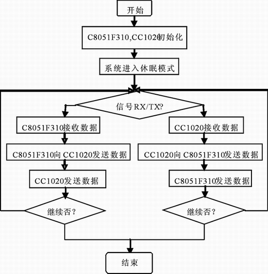
Figure 2 Main program flow diagram Software design
The communication protocol adopts UART format (a start bit, load data, and an end bit). In addition, there is a synchronization code in front of the data packet. The function of the synchronization code is to enable the receiving chip to correctly recognize the UART format data. After that, there must be an identification code, which is used to mark the beginning of the data. If the identification code is received correctly, it means that the data can be received correctly. If the data length is not constant, add a length code at the beginning of the data packet, or add a specific end mark at the end of the data packet. In order to cope with possible data errors in wireless transmission, add a check code at the end of the data packet, so that you can choose to drop the packet or request retransmission according to the application needs. In practical application, it is found that after the data packet, it is better to have a redundancy code of 1 ~ 2 bytes. Otherwise, the data of the last byte is easily susceptible to noise interference, causing false recognition. The main flow diagram is shown in Figure 2.
Conclusion
The communication module has the characteristics of low cost, strong versatility, strong expandability and high reliability. It can be used alone or integrated into various wireless measurement and control systems as a system expansion module.
Win 3 Cap Lamps are produced under IECEX quality control. The lamps are applied with IECEX explosive-proof certificates, build with brilliant electronic design and superior impact resistant, explosion-proof housing material, It is completely static proof and fire resistan.
The high quality LED has a lifespan of more than 30,000 hours and the phosphate technology battery up to 1000 cycles.
Small size and light weight, easy to carry
The highest ingress protection IP 68
Various application: coal miners, tunnel projects, oil fielda , camping, hiking, night fishing, night flying, sailing, etc.
Static Proof Cap Lamp Fire Resistant
Miners Lights For Hard Hats,Underground Mining Lights,Cordless Led Mining Cap Lights,Coal Miners Hard Hat With Light
ZHEJIANG HUACAI OPTIC-TECHNOLOGY CO LTD , https://www.win3safety.com