Digital frequency domain interference canceller based on Xilinx FPGA
Background of the project
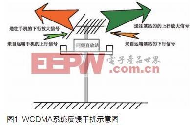
Repeaters are indispensable in modern communication systems, but if the transceiver antenna isolation of the repeater is insufficient and the overall gain is too large, the output signal will be fed back to the input after a delay, which will cause the repeater to output The signal is severely distorted and self-excited. In the same frequency repeater station of the wireless communication system, in order to reduce the product volume and shorten the cost of building a station, the transceiver antennas are often placed together (or very close). Because the receiving and transmitting antennas often only have different directional angles, the receiving antenna of the repeater will definitely receive the amplified signal sent by its repeating antenna and interfere with the desired useful signals. If the interference signal is not processed, the superimposed signal of the interference and the expected signal will be sent to the power amplifier again, and then amplified and forwarded. The intensity of the interference signal will always accumulate, eventually making the repeater unable to work normally. This positive feedback interference (the modulation parameters of the interference signal and the normal communication signal and the carrier frequency are completely consistent, so that the receiver receives the mixed signal with the same frequency interference superimposed) will also cause serious electromagnetic interference on digital communication, thus Impedes normal communication. This feedback interference often exists in the uplink and downlink, as shown in Figure 1.
Interference cancellation is a necessary technology for the same frequency repeater, and is also a very important subject in the field of signal processing [1]. Traditionally, the methods to overcome the self-excitation phenomenon are: (1) blocking the transmitting and receiving antennas with the help of buildings; (2) increasing the spatial isolation of the repeater ’s donor and retransmitting antennas. The vertical isolation is generally better than 1m, and the horizontal isolation can be more than ten meters. If there is no vertical isolation, the distance of horizontal isolation is almost 200 meters; (3) Reduce the gain of the repeater: the uplink and downlink are proportional, that is, the uplink and downlink are balanced until the self-excitation is eliminated.
Although the above three methods can reduce the impact of interference to a certain extent, in some occasions, these methods are not feasible due to environmental or system performance requirements. Therefore, using an adaptive interference canceller to reduce the co-channel feedback interference of repeater equipment has become the preferred solution. In all adaptive schemes, especially frequency domain algorithms achieve a good balance between performance and complexity.
This project takes the WCDMA system as an example to discuss the implementation of the digital frequency domain adaptive interference cancellation technology, and evaluates the program from performance indicators such as power spectral density and constellation diagram and error vector magnitude (EVM). In the design, in order to verify the performance of the algorithm and ensure the normal operation of the receiving end, at the same time, the three-step synchronization process of WCDMA cell search is realized, and the input and output data are compared and analyzed through a PC to verify the performance of the solution.
System solutions
The complete system starts from the baseband data after digital down-conversion and ends with the front-end of digital up-conversion, including the two major components of system synchronization and interference cancellation. The system block diagram is shown in Figure 2, and its brief introduction is as follows:
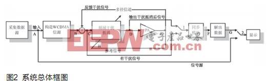
(1) In the case of no interference, the collected data source is input from point A, and then it is constructed as a WCDMA source as an input to the frequency domain interference cancellation module. In order to make the interference cancellation module operate correctly, the output signal at point B in this design is 4 samples per chip.
(2) To reflect the effect of frequency domain interference cancellation, an interference signal must be simulated in the system. This design uses the output of point D as the interference signal through the power amplifier (PA).
(3) Pass the interference signal through the multipath channel, feed it back to point B to superimpose with the WCDMA signal, and then enter the interference cancellation module. In order to cancel the interference, the output of point E is fed back to the interference cancellation module as a reference signal. In the following, this feedback branch is called the auxiliary link; and the link of interference cancellation + power amplifier is called the main link.
(4) The interfered signal passes through the frequency domain interference cancellation module, and outputs the canceled interference-free signal to the synchronization module, that is, point D. The synchronization module performs a three-step search to obtain the frame header and scrambling code information. After the desynchronized chip signal is descrambled and despread, information data is obtained, which is output as point G in the figure.
(5) At switch 1, you can choose: the signal with interference (point C) or the signal after interference cancellation (point D) is input to the synchronization module, and the output is displayed.
(6) At switch 2, you can choose: direct display of the data source (point A), or display of the data solved after synchronization (point G).
algorithm design
The frequency domain adaptive interference cancellation (AIC) module utilizes the LMS algorithm implemented in the frequency domain [2, 3]. The algorithm uses the fast Fourier transform (FFT) of the 1/2 overlap retention method to achieve fast correlation and fast convolution in the frequency domain by directly multiplying calculations [4]. The basic block diagram of the algorithm is shown in Figure 3, where point A is the interfered signal, B is the signal of the feedback link, and point C is the output after the interference is cancelled. It mainly includes the following cyclically executed operation flow, where k represents the k-th data block:
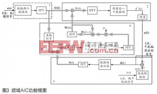
(1) Initially set the M frequency-domain tap coefficients W (k) of the adaptive filter;
(2) The time-domain continuous input signal u (n) of the filter is composed of each M, and then two data blocks are cascaded to perform N-point discrete fast Fourier transform to convert it into a frequency domain signal U (k) And use this signal as the input of the adaptive filter; where N is twice the number of taps M of the filter, that is, N = 2M;
(3) U (k) is filtered to obtain the output signal Y (k), and then inverse fast Fourier transform (IFFT) processing is performed to convert it into a time-domain signal y (k) as an estimated value of interference;
(4) Calculate the difference between the interfered signals r (k) and y (k), which is the signal d (k) after interference cancellation; the frequency domain value D (k) that generates the desired signal is the next filter Used for iterative tap coefficients;
(5) Use the frequency domain signal to calculate the minimum mean square error LMS, that is, update W (k) according to D (k) and U (k), and return the updated value to step (2). Jump to step (2) and iterate repeatedly until the interference is cancelled.
Compared with the traditional time-domain LMS algorithm, the frequency-domain LMS algorithm can reduce the computational complexity. Assuming that the input is a real signal, the number of filter taps is. It can be obtained that the ratio of the computational complexity of the frequency domain LMS and the time domain LMS is 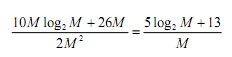 . In practice, the delay of interference transmission in the air will be much larger than the delay of the feedback signal. At this time, a larger number of taps is required to cancel the interference. Assuming M = 1024, the frequency-domain LMS algorithm can be increased by approximately 16 times faster than the time-domain LMS algorithm. For the sake of simplicity, in this document, M = 64 is adopted, and the frequency domain LMS algorithm is used, and the calculation amount can be about 1.5 times faster than the time domain LMS algorithm.
WCDMA synchronization algorithm
For any system, the normal operation must first ensure the synchronization of the system. WCDMA cell search is divided into three stages, namely primary synchronization, secondary synchronization and pilot search [5]. The primary synchronization uses the PSC code to correlate the received primary synchronization channel data (PSCH), and determines the slot header according to the position of the correlation peak. After the primary synchronization is completed, the secondary synchronization phase can determine the frame header position and the scrambling code group number used by the current cell. The method is to use the secondary synchronization code (SSC) to do the correlation. The last stage is the pilot search, using the scrambling code group number and frame header information that have been obtained, to traverse all 8 possible primary scrambling codes of a main scrambling code group, which are respectively related to the pilot channel (CPICH). The scrambling code number is finally determined according to the largest correlation value. It can be seen that after the three-step synchronization of WCDMA, the main scrambling code number and frame synchronization information of the current cell can be obtained. The flowchart of the three-step synchronization is shown in Figure 4.
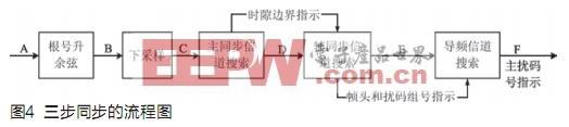
Since the signal received by the synchronization module is 4 samples, and the search process within the synchronization module only needs to use single-sampled data, the oversampled signal must be down-sampled first. In addition, in order to match the transmitted signal source, the received signal is first passed through a root-raised cosine matched filter, and then down-sampled to the chip rate, as shown in point B.
Simulation and test results
Simulation results
First of all, after power spectrum density map (PSD) verification, the output signal PSD curve after AIC is basically the same as the transmission source PSD curve. Figure 5 shows the fixed-point simulation results of the algorithm when the signal-to-interference ratio is -10dB.
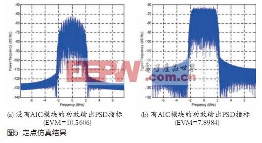
Specifically, in the absence of AIC, the fluctuation of the main lobe of the output signal spectrum is large, and the dB value of the main lobe decreases. After adopting AIC, the fluctuations in the main lobe of the output signal spectrum are basically improved, and the decreasing dB value is basically equal to the decreasing dB value of the original input source, indicating that the AIC performance is good.
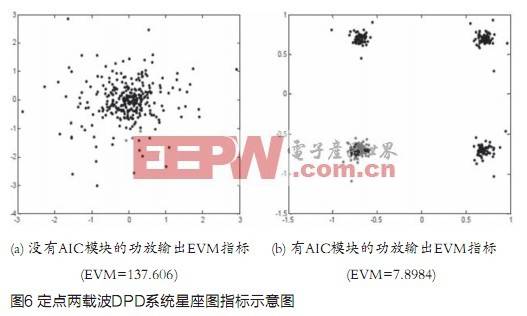
Second, by comparing the quantization index EVM [3], Figure 6 shows the EVM index when the signal-to-interference ratio is -10dB. It can be seen that the AIC algorithm can effectively cancel interference and improve the constellation diagram.
Hardware test instructions
In hardware implementation, the development platform used is Virtex II Board. Among them, V2P30 chip FPGA has 136 hard core multipliers and block RAM, which can meet the needs of a large number of multipliers and memory for adaptive filtering algorithms and large-point FFT transformation. In addition, a large number of slices can realize the establishment of cell search modules and related test platforms.
In addition, for a simple video test platform, use the VGA interface to complete the test platform for final test verification. XUP Virtex II PRO board with high-precision DAC chip FMS3818, can achieve the intended purpose. The software development selected ISE8.2.03i, and the corresponding Chipscope is version 8.2.
The hardware system needs to implement four major modules: frequency domain AIC, cell synchronous search, WCDMA source generator, and test platform. The AIC module can be divided into large-point FFT transformation and corresponding serial-parallel, parallel-serial conversion and other main functions. The design is divided into 5 large modules: top-level module, AIC processing module, source generator, cell search and test platform. The FFT module is completed using Xilinx's IP Core (intellectual property core); serial-parallel and parallel-serial can be implemented using block RAM; the data processing module is implemented using the SRL16 structure as much as possible to save resources.
The system test is completed according to the idea from part to whole. First, each module is tested separately, then some modules are combined to complete the test, and finally the whole system is tested. In this way, errors can be discovered early and eliminated at the initial stage. The test mainly relies on ChipScope to complete the data collection, and then imports the data into MATLAB, compares it with fixed-point simulation and ModelSim output results, and completes data analysis to ensure that the chip's operating results and simulation results are the same. In the test, all were based on the square wave test platform.
This Wifi Backup Camera connects wirelessly to your smartphone allowing you to see the camera view on your smartphone screen! Download the free My Cam app from the App Store for IOS device or Google Play Store for Android device , the camera and smartphone will be able to connect via a WiFi connection .
1, Wifi Wireless Backup Camera system for Truck/Van/Caravan/Trailers/Camper/Pickup/5th Wheel/Bus. Easy to install, no more complex wiring.
2,Rearview IR Reverse HD backup Camera with Built-in Wireless Transmitter---with 12/18/28 individual Infrared (IR) LED for Night Vision. Hard Metal Cased Camera with IP68 Waterproof and Mud proof, Designed and tested for extreme climates.
3, Voltage Range From 12-32V DC Power, Flexible Vehicle Compatibility.
4, Digital wireless technology for specialty vehicles , No any interference with other wireless devices, if you ensure stable and high resolution image with 100M acceptance range in open areas.
Wifi Backup Camera
Wifi Backup Camera,Wifi Wireless Backup Camera,Wifi Wireless Backup Camera For Suv,Wifi Plate Frame Backup Camera
Shenzhen Sunveytech Co.,LTD , https://www.sunveytech.com