Abstract: Compared with a typical "local" clock scheme, the integrated multi-output clock generator has many advantages. This article discusses the advantages of centralized clock generators (such as MAX9489 and MAX9471), such as: reducing system cost, good signal integrity, suppressing interference, etc., also gives the relevant content of circuit board design, discusses the use of centralized clock source design The basic problems faced at the time.
The MAX9489 / MAX9471 are multi-output clock generators, the MAX9489 is designed for SOHO routers and network equipment, and the MAX9471 is designed for consumer electronics.
Compared with a typical "local" clock scheme, a centralized clock generator can provide more advantages for multi-port, multi-module applications.
There are some practical issues to consider when using multi-output clock generators. The guidelines given here help to improve the design of centralized clock sources, eliminate adverse effects on signals, eliminate noise interference, and reduce system costs. This article uses a block diagram to illustrate these applications.
Application advantages of centralized clock source The existing network router / switch system must support more and more connection ports and modules. Each port or module generally requires a reference clock. This clock is usually made by the local crystal associated with the port or module. Or crystal oscillator provided. As the number of ports or modules increases, the cost of the reference clock also increases. Moreover, this local clock scheme makes it very difficult for the system to reconfigure the reference clock for testing, and is not suitable for interface power management and port (or module) upgrade or downgrade. This is exactly the design challenge faced by set-top boxes and digital TVs.
Centralized clock generator is not a new concept, it has been widely used in PC motherboards. For example, in a set-top box design, there are more than 11 different interfaces or modules, which require different clocks. The MAX9489 can generate all the clocks needed by routers and set-top boxes without providing a local reference clock. Using an integrated multi-output clock generator such as the MAX9489 and MAX9471 can save system costs and improve the design's ability to control the system.
The MAX9489 provides 15 LVCMOS programmable clock outputs. Each clock has 10 different frequency options, suitable for Ethernet, PCI, memory, and MCU. In the MAX9489, each clock can be individually controlled through the I²C interface. In addition, the clock output frequency of the MAX9489 can be adjusted up or down by 5% or 10%, which facilitates overdrive and underdrive test of the system. In order to reduce EMI, we also integrated spread spectrum and slew rate control functions in the MAX9489. Figure 1 and Figure 2 show the application block diagram of MAX9489 in routers and the application block diagram of MAX9471 in set-top boxes, respectively.
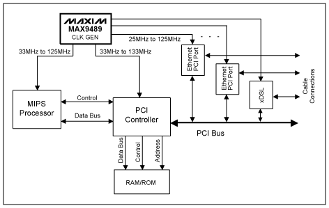
Figure 1. Block diagram of the SOHO router system
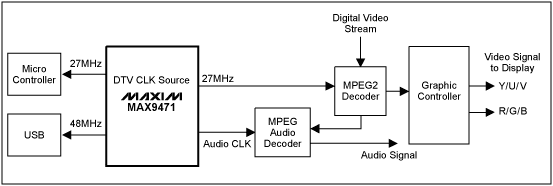
Figure 2. Block diagram of a set-top box system. When designing a circuit board with an integrated clock generator, how to solve the clock cross-board connection without reducing signal integrity is a design challenge. Generally, the length of the clock lead is between 3 inches and 9 inches. For such a lead length, according to the design principle of the motherboard, the LVCMOS signal can work up to 150MHz. However, circuit board layout must be carefully considered. Two practical issues need to be resolved: the effect of longer PCB leads on rise / fall times must be reduced, and in addition, noise interference from other signal sources on the same circuit board must be eliminated.
Reducing the effect on the signal To reduce the effect on the signal rise / fall time, a 50Ω lead is often used, and a 25Ω to 33Ω resistor (Rs) is inserted between the CLK output pin and the lead. It is known that the impedance of the pull-up and pull-down transistors of the driver is about 20Ω. Inserting Rs can match the total output impedance of the LVCMOS driver to the 50Ω lead. The schematic diagram of the driver circuit is shown in Figure 3.
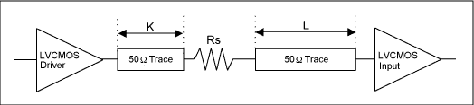
Figure 3. LVCMOS output drive circuit
Table 1 gives the lengths of K and L.
Table 1. LVCMOS clock wiring length
The resistor Rs should be connected to the LVCMOS output pin through the K-inch lead. The optimal values ​​of K and Rs can be determined by experiment or simulation. These values ​​are a function of the driver's output impedance, lead impedance and length, and are also related to actual components and terminal impedance. If the distance between the output pin and the terminal is less than 2 inches, you do not need to use Rs. When the clock frequency is higher than 100MHz, the clock lead length should be further reduced. To illustrate that matching leads can provide better signal integrity, we used the MAX9489 to generate a 100MHz clock and connect it to a 5-inch long 50Ω lead. Figure 4 shows the waveforms tested at different positions of the leads.
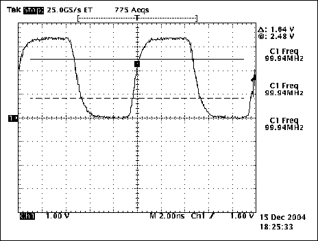
Figure 4. Waveform of LVCMOS output pin without leads
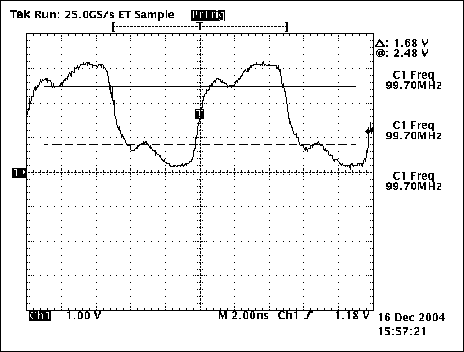
Figure 5. The waveform when the terminal has a 5-inch lead, Rs = 0Ω
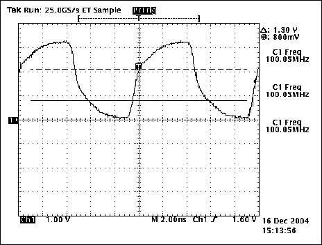
Figure 6. The waveform when the terminal has a 5-inch lead, Rs = 33Ω, K = 0.5 inch
As shown in Figures 4 to 6, by increasing Rs at an appropriate location, the signal integrity is effectively improved.
Avoiding noise interference In order to solve the second practical problem of noise interference, we need to reduce the mutual interference between the clock and other signals. The clock lead is preferably sandwiched between ground wires, as shown in Figure 7.
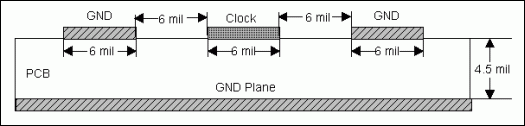
Figure 7. Clock routing with ground isolation
The MAX9489 / MAX9471 are multi-output clock generators, the MAX9489 is designed for SOHO routers and network equipment, and the MAX9471 is designed for consumer electronics.
Compared with a typical "local" clock scheme, a centralized clock generator can provide more advantages for multi-port, multi-module applications.
There are some practical issues to consider when using multi-output clock generators. The guidelines given here help to improve the design of centralized clock sources, eliminate adverse effects on signals, eliminate noise interference, and reduce system costs. This article uses a block diagram to illustrate these applications.
Application advantages of centralized clock source The existing network router / switch system must support more and more connection ports and modules. Each port or module generally requires a reference clock. This clock is usually made by the local crystal associated with the port or module. Or crystal oscillator provided. As the number of ports or modules increases, the cost of the reference clock also increases. Moreover, this local clock scheme makes it very difficult for the system to reconfigure the reference clock for testing, and is not suitable for interface power management and port (or module) upgrade or downgrade. This is exactly the design challenge faced by set-top boxes and digital TVs.
Centralized clock generator is not a new concept, it has been widely used in PC motherboards. For example, in a set-top box design, there are more than 11 different interfaces or modules, which require different clocks. The MAX9489 can generate all the clocks needed by routers and set-top boxes without providing a local reference clock. Using an integrated multi-output clock generator such as the MAX9489 and MAX9471 can save system costs and improve the design's ability to control the system.
The MAX9489 provides 15 LVCMOS programmable clock outputs. Each clock has 10 different frequency options, suitable for Ethernet, PCI, memory, and MCU. In the MAX9489, each clock can be individually controlled through the I²C interface. In addition, the clock output frequency of the MAX9489 can be adjusted up or down by 5% or 10%, which facilitates overdrive and underdrive test of the system. In order to reduce EMI, we also integrated spread spectrum and slew rate control functions in the MAX9489. Figure 1 and Figure 2 show the application block diagram of MAX9489 in routers and the application block diagram of MAX9471 in set-top boxes, respectively.
Figure 1. Block diagram of the SOHO router system
Figure 2. Block diagram of a set-top box system. When designing a circuit board with an integrated clock generator, how to solve the clock cross-board connection without reducing signal integrity is a design challenge. Generally, the length of the clock lead is between 3 inches and 9 inches. For such a lead length, according to the design principle of the motherboard, the LVCMOS signal can work up to 150MHz. However, circuit board layout must be carefully considered. Two practical issues need to be resolved: the effect of longer PCB leads on rise / fall times must be reduced, and in addition, noise interference from other signal sources on the same circuit board must be eliminated.
Reducing the effect on the signal To reduce the effect on the signal rise / fall time, a 50Ω lead is often used, and a 25Ω to 33Ω resistor (Rs) is inserted between the CLK output pin and the lead. It is known that the impedance of the pull-up and pull-down transistors of the driver is about 20Ω. Inserting Rs can match the total output impedance of the LVCMOS driver to the 50Ω lead. The schematic diagram of the driver circuit is shown in Figure 3.
Figure 3. LVCMOS output drive circuit
Table 1 gives the lengths of K and L.
Table 1. LVCMOS clock wiring length
| K | L | |
| Trace Length at 33MHz | 0.1 to 1.0 inches | 2 to 13 inches |
| Trace Length at 100MHz | 0.1 to 1.0 inches | 2 to 9 inches |
The resistor Rs should be connected to the LVCMOS output pin through the K-inch lead. The optimal values ​​of K and Rs can be determined by experiment or simulation. These values ​​are a function of the driver's output impedance, lead impedance and length, and are also related to actual components and terminal impedance. If the distance between the output pin and the terminal is less than 2 inches, you do not need to use Rs. When the clock frequency is higher than 100MHz, the clock lead length should be further reduced. To illustrate that matching leads can provide better signal integrity, we used the MAX9489 to generate a 100MHz clock and connect it to a 5-inch long 50Ω lead. Figure 4 shows the waveforms tested at different positions of the leads.
Figure 4. Waveform of LVCMOS output pin without leads
Figure 5. The waveform when the terminal has a 5-inch lead, Rs = 0Ω
Figure 6. The waveform when the terminal has a 5-inch lead, Rs = 33Ω, K = 0.5 inch
As shown in Figures 4 to 6, by increasing Rs at an appropriate location, the signal integrity is effectively improved.
Avoiding noise interference In order to solve the second practical problem of noise interference, we need to reduce the mutual interference between the clock and other signals. The clock lead is preferably sandwiched between ground wires, as shown in Figure 7.
Figure 7. Clock routing with ground isolation
VFD power cable
Product Name: 0.6/1kV low smoke halogen free VFD power cable
Model: TFOU(C)-VFD
Specification: 3×1.5+3×1.0/3mm2~3×185+3×95/3mm2
Executive Standards: IEC60092-350, Q/321001KLA089-2007
Application: The cable is cable specifically engineered for use in variable frequency AC motor drive (VFD) applications.
Low Voltage Marine Vfd Power Cable
Low Voltage Cable,Low Voltage Marine Vfd Power Cable,Low Voltage Shipboard Vdf Power Cable,Low Voltage Power Cable
Jiangsu Jiangyang Special Cable Co,.Ltd. , https://www.jymarinecable.com